 Deutsch
 English
 Español
 Français
 Italiano
 Nederlands
 Polski
 Português
 Русский
 Türkçe
 Svenska
 Chinese
 Magyar
Intel Core i5-12600K vs Intel Core i7-4578U
Intel Core i5-12600K
► remove from comparison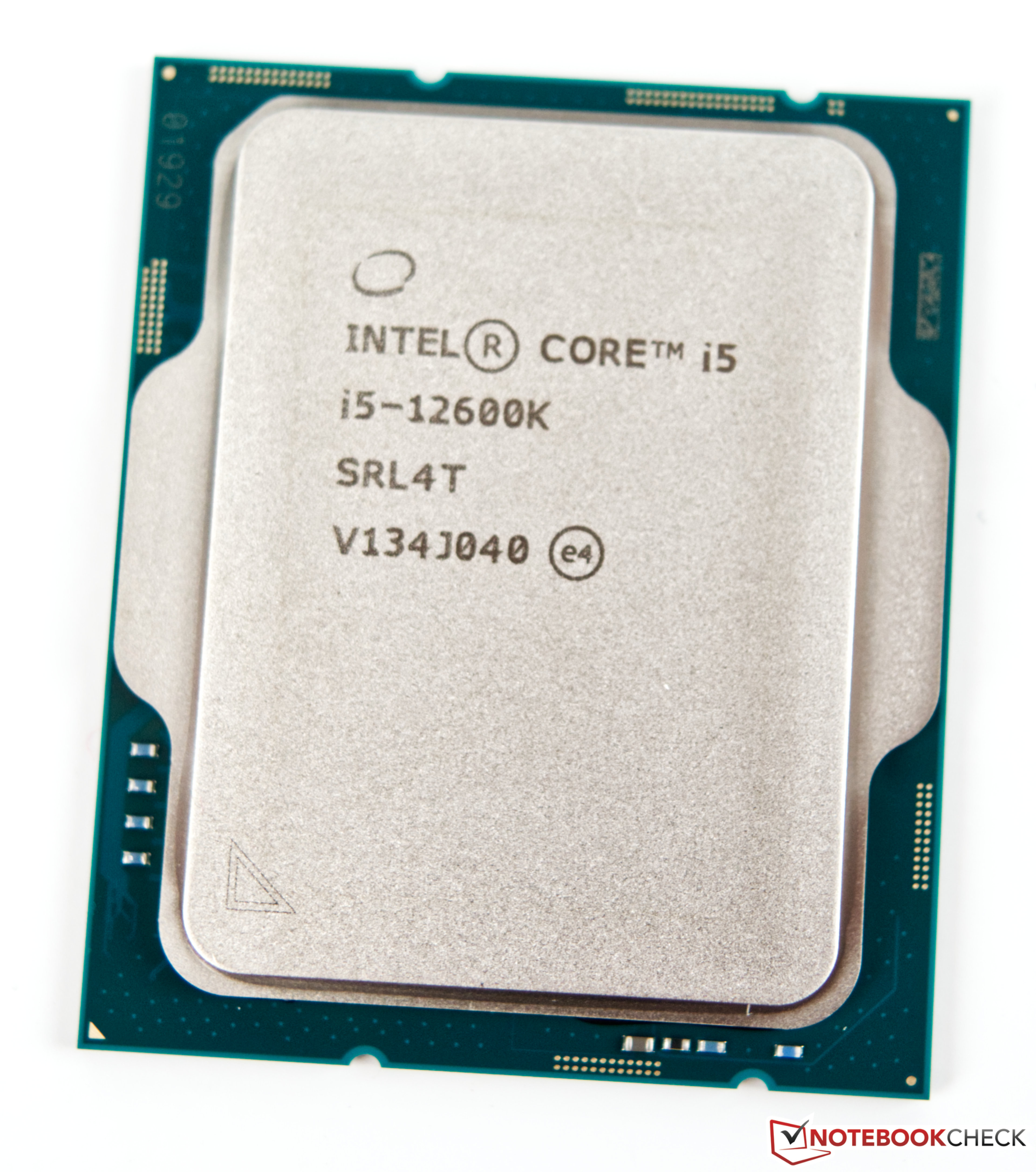
The Intel Core i5-12600K is a mid-range CPU for desktops based on the Alder Lake architecture. It was first announced in November 2021 and offers 6 performance cores and 4 efficiency cores. The performance cores (P-cores) support HyperThreading, leading to 16 Threads that can be processed at once. The performance cores can clock with up to 4.9 GHz, the efficiency cores can clock with up to 3.6 GHz. All cores can use 20 MB Smart Cache. The integrated memory controller supports up to 128 GB DDR5 with 4800 MT/s (dual channel).
Thread Director (in hardware) can support the operating system to decide which thread to use on the performance or efficiency cores for the best performance.
The integrated graphics adapter is based on the Xe-architecture and called Intel UHD Graphics 770. It clocks between 300 and 1.45 GHz.
For AI tasks, the CPU also integrates GNA 3.0 and DL Boost. Quick Sync in version 8 is the same as in the Rocket Lake CPUs and supports MPEG-2, AVC, VC-1 decode, JPEG, VP8 decode, VP9, HEVC and AV1 decode in hardware.
Performance
The average 12600K in our database is way ahead of the Ryzen 9 3900 and the Core i9-10900K, as far as multi-thread benchmark scores are concerned. This is a very fast CPU that should have no trouble running triple-A games for at least a couple of years.
Power consumption
This Core i5 series chip has a Base power consumption of 125 W, with its maximum Intel-recommended Turbo power consumption sitting at 150 W.
The i5-12600K is built with Intel's fourth generation 10 nm process marketed as Intel 7 for lower-than-average, as of mid 2023, energy efficiency.
Intel Core i7-4578U
► remove from comparisonThe Intel Core i7-4578U is a LV (low voltage) dual-core processor for large ultrabooks launched in Q3/2014. It is based on the Haswell architecture and is manufactured in 22nm. Due to Hyper-Threading, the two cores can handle up to four threads in parallel, leading to better utilization of the CPU. Each core offers a base speed of 3.0 GHz, but can dynamically increase clock rates with Turbo Boost up to 3.5 GHz.
Architecture
Haswell is the successor to the Ivy Bridge architecture with improvements on both GPU and CPU performance. The CPUs are produced in 22nm and offer an optimized branch prediction as well as additional execution ports, improving the performance per clock by almost 10 percent. Furthermore, new features like AVX2 and FMA should increase the performance in future applications.
Performance
The performance of the Core i7-4578U is slightly above the older and somewhat higher clocked Core i7-3540M. However, when using new instruction sets such as AVX2 the performance can be significantly better. Thus, the CPU has sufficient power for office and multimedia purposes as well as more demanding applications.
Graphics
The integrated Iris Graphics 5100 offers 40 Execution Units (EUs) clocked at 200 - 1200 MHz with Turbo Boost, making it significantly faster than the HD Graphics 4000. As a result, the Iris Graphics competes with dedicated lower mid-range graphics cards (e.g. GeForce GT 720M).
Power Consumption
The i7-4578U is rated at a TDP of 28 W including the graphics card, memory controller, VRMs and the integrated chipset. Therefore, the CPU is suited for larger, well-cooled ultrabooks.
| Model | Intel Core i5-12600K | Intel Core i7-4578U | ||||||||||||||||||||||||||||||||||||||||||||||||||||||||||||||||||||||||||||||||||||||||||||||||||||||||||||||||||||||||||||||||||||||||||||||||||||||||||||||||||||
| Series | Intel Alder Lake-S | Intel Core i7 | ||||||||||||||||||||||||||||||||||||||||||||||||||||||||||||||||||||||||||||||||||||||||||||||||||||||||||||||||||||||||||||||||||||||||||||||||||||||||||||||||||||
| Codename | Alder Lake | Haswell | ||||||||||||||||||||||||||||||||||||||||||||||||||||||||||||||||||||||||||||||||||||||||||||||||||||||||||||||||||||||||||||||||||||||||||||||||||||||||||||||||||||
| Series: Core i7 Haswell |
|
| ||||||||||||||||||||||||||||||||||||||||||||||||||||||||||||||||||||||||||||||||||||||||||||||||||||||||||||||||||||||||||||||||||||||||||||||||||||||||||||||||||||
| Clock | 2800 - 4900 MHz | 3000 - 3500 MHz | ||||||||||||||||||||||||||||||||||||||||||||||||||||||||||||||||||||||||||||||||||||||||||||||||||||||||||||||||||||||||||||||||||||||||||||||||||||||||||||||||||||
| L2 Cache | 9.5 MB | 512 KB | ||||||||||||||||||||||||||||||||||||||||||||||||||||||||||||||||||||||||||||||||||||||||||||||||||||||||||||||||||||||||||||||||||||||||||||||||||||||||||||||||||||
| L3 Cache | 20 MB | 4 MB | ||||||||||||||||||||||||||||||||||||||||||||||||||||||||||||||||||||||||||||||||||||||||||||||||||||||||||||||||||||||||||||||||||||||||||||||||||||||||||||||||||||
| Cores / Threads | 10 / 16 | 2 / 4 | ||||||||||||||||||||||||||||||||||||||||||||||||||||||||||||||||||||||||||||||||||||||||||||||||||||||||||||||||||||||||||||||||||||||||||||||||||||||||||||||||||||
| TDP | 125 Watt | 28 Watt | ||||||||||||||||||||||||||||||||||||||||||||||||||||||||||||||||||||||||||||||||||||||||||||||||||||||||||||||||||||||||||||||||||||||||||||||||||||||||||||||||||||
| Technology | 10 nm | 22 nm | ||||||||||||||||||||||||||||||||||||||||||||||||||||||||||||||||||||||||||||||||||||||||||||||||||||||||||||||||||||||||||||||||||||||||||||||||||||||||||||||||||||
| max. Temp. | 100 °C | 100 °C | ||||||||||||||||||||||||||||||||||||||||||||||||||||||||||||||||||||||||||||||||||||||||||||||||||||||||||||||||||||||||||||||||||||||||||||||||||||||||||||||||||||
| Socket | LGA1700 | FCBGA | ||||||||||||||||||||||||||||||||||||||||||||||||||||||||||||||||||||||||||||||||||||||||||||||||||||||||||||||||||||||||||||||||||||||||||||||||||||||||||||||||||||
| Features | DDR4-3200/DDR5-4800 RAM, PCIe 5, Thr. Dir., DL Boost, GNA, vPro Enterp., MMX, SSE, SSE2, SSE3, SSSE3, SSE4.1, SSE4.2, AVX, AVX2, BMI2, ABM, FMA, ADX, SMEP, SMAP, EIST, TM1, TM2, HT, Turbo, SST, AES-NI, RDRAND, RDSEED, SHA | Iris Graphics 5100 (200 - 1200 MHz), DDR3(L)-1600 Memory Controller, HyperThreading, AVX, AVX2, Quick Sync, Virtualization, AES-NI | ||||||||||||||||||||||||||||||||||||||||||||||||||||||||||||||||||||||||||||||||||||||||||||||||||||||||||||||||||||||||||||||||||||||||||||||||||||||||||||||||||||
| iGPU | Intel UHD Graphics 770 (300 - 1450 MHz) | Intel Iris Graphics 5100 (200 - 1200 MHz) | ||||||||||||||||||||||||||||||||||||||||||||||||||||||||||||||||||||||||||||||||||||||||||||||||||||||||||||||||||||||||||||||||||||||||||||||||||||||||||||||||||||
| Architecture | x86 | x86 | ||||||||||||||||||||||||||||||||||||||||||||||||||||||||||||||||||||||||||||||||||||||||||||||||||||||||||||||||||||||||||||||||||||||||||||||||||||||||||||||||||||
| $289 U.S. | $426 U.S. | |||||||||||||||||||||||||||||||||||||||||||||||||||||||||||||||||||||||||||||||||||||||||||||||||||||||||||||||||||||||||||||||||||||||||||||||||||||||||||||||||||||
| Announced | ||||||||||||||||||||||||||||||||||||||||||||||||||||||||||||||||||||||||||||||||||||||||||||||||||||||||||||||||||||||||||||||||||||||||||||||||||||||||||||||||||||||
| Manufacturer | ark.intel.com | ark.intel.com | ||||||||||||||||||||||||||||||||||||||||||||||||||||||||||||||||||||||||||||||||||||||||||||||||||||||||||||||||||||||||||||||||||||||||||||||||||||||||||||||||||||
| L1 Cache | 128 KB | |||||||||||||||||||||||||||||||||||||||||||||||||||||||||||||||||||||||||||||||||||||||||||||||||||||||||||||||||||||||||||||||||||||||||||||||||||||||||||||||||||||
| Transistors | 1300 Million | |||||||||||||||||||||||||||||||||||||||||||||||||||||||||||||||||||||||||||||||||||||||||||||||||||||||||||||||||||||||||||||||||||||||||||||||||||||||||||||||||||||
| Die Size | 181 mm2 |
