 Deutsch
 English
 Español
 Français
 Italiano
 Nederlands
 Polski
 Português
 Русский
 Türkçe
 Svenska
 Chinese
 Magyar
AMD Radeon R9 M470X vs Intel HD Graphics 510 vs AMD Radeon R9 M470
AMD Radeon R9 M470X
► remove from comparisonThe AMD Radeon R9 M470X is an upper mainstream mobile graphics card based on the familiar Bonaire chip. This 28 nm GPU uses all 896 shaders (14 Compute Units CU) and is based on the second generation of the GCN architecture (Graphics Core Next). The maximum memory size is 4 GB (GDDR5, 6000 MHz effective) and it is attached via 128-bit interface. Compared to the technologically identical predecessor card Radeon R9 M385X (1100 MHz), the R9 M470X could have a slightly higher clock.
Contrary to the R9 M300 series, the number of products within the R9 M400 series is currently limited to three (M485X, M470X and M470), but this will probably change with the launch of the new Polaris architecture in Q2 2016.
Intel HD Graphics 510
► remove from comparison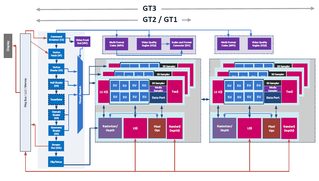
The Intel HD Graphics 510 (GT1) is an integrated graphics unit, which can be found in low-end ULV (Ultra Low Voltage) processors of the Skylake generation. This "GT1" version of the Skylake GPU offers 12 Execution Units (EUs) clocked at up to 950 MHz (depending on the CPU model). Due to its lack of dedicated graphics memory or eDRAM cache, the HD 510 has to access the main memory (2x 64bit DDR3L-1600 / DDR4-2133).
Performance
Depending on various factors like memory configuration, the HD Graphics 510 should perform sligthly below the older HD Graphics 4400 and will handle modern games (as of 2015) only in lowest settings (if it does at all).
Features
The revised video engine now decodes H.265/HEVC completely in hardware and thereby much more efficiently than before. Displays can be connected via DP 1.2 / eDP 1.3 (max. 3840 x 2160 @ 60 Hz), whereas HDMI is limited to the older version 1.4a (max. 3840 x 2160 @ 30 Hz). However, HDMI 2.0 can be added using a DisplayPort converter. Up to three displays can be controlled simultaneously.
Power Consumption
The HD Graphics 510 can be found in mobile processors specified at 15 W TDP and is therefore suited for compact laptops and ultrabooks.
AMD Radeon R9 M470
► remove from comparisonThe AMD Radeon R9 M470 is an upper mainstream mobile graphics card based on the familiar Bonaire chip. This 28 nm GPU uses 768 shaders (12 Compute Units CU) and is based on the second generation of the GCN architecture (Graphics Core Next). The maximum memory size is 4 GB (GDDR5, 6000 MHz effective) and it is attached via 128-bit interface. Compared to the technologically identical predecessor card Radeon R9 M380 (1000 MHz), the R9 M470 could have a slightly higher clock.
Contrary to the R9 M300 series, the number of products within the R9 M400 series is currently limited to three (M485X, M470X and M470), but this will probably change with the launch of the new Polaris architecture in Q2 2016.
| AMD Radeon R9 M470X | Intel HD Graphics 510 | AMD Radeon R9 M470 | |||||||||||||||||||||||||||||||||||||||||||||||||||||||||||||
| Radeon R9 M400 Series |
|
|
| ||||||||||||||||||||||||||||||||||||||||||||||||||||||||||||
| Architecture | GCN 2 | Gen. 9 Skylake | GCN 2 | ||||||||||||||||||||||||||||||||||||||||||||||||||||||||||||
| Pipelines | 896 - unified | 12 - unified | 768 - unified | ||||||||||||||||||||||||||||||||||||||||||||||||||||||||||||
| Core Speed | 1100 MHz | 300 - 950 (Boost) MHz | 1000 MHz | ||||||||||||||||||||||||||||||||||||||||||||||||||||||||||||
| Shader Speed | 6000 MHz | 6000 MHz | |||||||||||||||||||||||||||||||||||||||||||||||||||||||||||||
| Memory Speed | 6000 MHz | 6000 MHz | |||||||||||||||||||||||||||||||||||||||||||||||||||||||||||||
| Memory Bus Width | 128 Bit | 64/128 Bit | 128 Bit | ||||||||||||||||||||||||||||||||||||||||||||||||||||||||||||
| Memory Type | GDDR5 | DDR3/DDR4 | GDDR5 | ||||||||||||||||||||||||||||||||||||||||||||||||||||||||||||
| Max. Amount of Memory | 4 GB | 4 GB | |||||||||||||||||||||||||||||||||||||||||||||||||||||||||||||
| Shared Memory | no | yes | no | ||||||||||||||||||||||||||||||||||||||||||||||||||||||||||||
| API | DirectX 12 FL11_1, Shader 5.0, OpenGL 4.3 | DirectX 12_1, OpenGL 4.4 | DirectX 12 FL11_1, Shader 5.0, OpenGL 4.3 | ||||||||||||||||||||||||||||||||||||||||||||||||||||||||||||
| Transistors | 1.5 Billion | 1.5 Billion | |||||||||||||||||||||||||||||||||||||||||||||||||||||||||||||
| technology | 28 nm | 14 nm | 28 nm | ||||||||||||||||||||||||||||||||||||||||||||||||||||||||||||
| Features | DirectCompute 5.0, OpenCL | QuickSync | DirectCompute 5.0, OpenCL | ||||||||||||||||||||||||||||||||||||||||||||||||||||||||||||
| Notebook Size | large | large | |||||||||||||||||||||||||||||||||||||||||||||||||||||||||||||
| Date of Announcement | 14.05.2016 | 01.09.2015 | 14.05.2016 | ||||||||||||||||||||||||||||||||||||||||||||||||||||||||||||
| Link to Manufacturer Page | www.amd.com | www.amd.com | |||||||||||||||||||||||||||||||||||||||||||||||||||||||||||||
| Codename | Skylake GT1 | Saturn |
| ||||||||||||||||||


