 Deutsch
 English
 Español
 Français
 Italiano
 Nederlands
 Polski
 Português
 Русский
 Türkçe
 Svenska
 Chinese
 Magyar
AMD Ryzen 7 4980U vs Intel Pentium Silver J5040
AMD Ryzen 7 4980U
► remove from comparison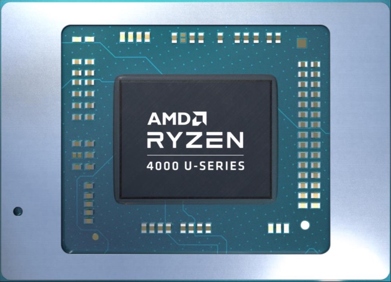
The AMD Ryzen 7 4980U is a Renoir family processor designed for certain Microsoft Surface systems. 4980U has eight Zen 2 cores clocked at 2.0 GHz (base clock speed) to 4.4 GHz (Boost) with thread-doubling SMT tech enabled for a total of 16 threads. The chip is manufactured on the modern 7 nm TSMC process and partly thanks to that AMD promises a 2x improvement in performance-per-Watt over Ryzen 3000 series mobile CPUs.
Architecture
The Zen 2 microarchitecture has brought a sizeable per-thread performance boost compared to the outgoing Zen+ parts. Renoir product family is also the first to introduce 8-core ULV processors to laptop market, keeping power consumption within reasonable limits. This AMD processor family is very impressive from most perspectives. One of the disatvantages to keep in mind is the lack of PCI-Express 4 support, meaning these blazing-fast NVMe SSDs will be limited to 3.9 GB/s tops.
Ryzen 7 4980U is designed to work with quad-channel LPDDR4 memory at up to 4,267 MHz. 8 MB of Level 3 are present in this chip. The Ryzen 7 gets soldered straight to the motherboard (FP6 socket) and is thus not user-replaceable. Please go to our Renoir hub page for more information on the product family.
Performance
The 4980U is the fastest U-class Ryzen 4000 series chip. As such, its clock speeds are 200 MHz higher (both the base one and Boost one) than what the Ryzen 7 4800U has.
It is thus hardly surprising that the average 4980U in our database is in the same league as the Ryzen 7 5800U and also the Core i7-1260P, as far as multi-thread benchmark scores are concerned.
Graphics
In addition to its eight CPU cores, the Ryzen 7 also features the Radeon RX Vega 8 graphics adapter with 8 CUs (= 512 shaders) at up to 1,950 MHz. This iGPU is compatible with FreeSync and DirectX 12 and is able to HW-decode AVC, HEVC, VP9-encoded videos (no AV1 support here). Vega 8 is capable of outputting UHD 2160p60 video signal to several monitors and, similar to Intel's Iris Xe (80 EUs), is good enough for a bit of light gaming on the go, provided one is content with sub-1080p resolutions and low/medium quailty presets.
Power consumption
The APU has a default TDP, also known as the long-term power limit, of 15 W; much like it is with other U-class Ryzen 4000 chips, AMD is fine with laptop makers (Microsoft, in this case) changing that value to anything between 10 W and 25 W.
The 7 nm TSMC process this Ryzen 7 is built with makes for above average, as of mid 2022, energy efficiency.
Intel Pentium Silver J5040
► remove from comparisonThe Intel Pentium Silver J5040 is a quad-core SoC primarily for inexpensive mini-PCs and was announced late 2019. It runs at 2 GHz (base) to 3.2 GHz (single core burst) and is based on the Gemini Lake platform (refresh). Similar to the Apollo Lake predecessor, the chip is manufactured in a 14 nm process with FinFETs but offers slightly improved processor cores, double the amount of L2 cache, a smaller package, a better GPU architecture and a partly integrated WiFi support. Besides four CPU cores, the chip also includes a DirectX 12 capable GPU as well as a DDR4/LPDDR4 memory controller (dual-channel, up to 2400 MHz). The SoC is not replaceable as it is directly soldered to the mainboard.
Architecture
The processor architecture is still called Goldmont Plus. Compared to the older Goldmont cores in Apollo Lake, they feature an increased level 2 cache (to 4 MB). That means the per-clock-performance should be a bit better, but not near the Core CPUs like Kaby Lake Y.
Performance
Thanks to the higher clock speed and TDP, the Pentium J5040 is slightly faster than the mobile counterpart, the Pentium Silver N5030. Compare to AMD, it ranks on average slightly higher compared to the Athlon Silver 3050e (Zen based Dual-Core) that wins in single-core tests but looses out in multi-threaded tests. Intel Core i3 from 2019 (like the i3-1005G1) are clearly faster and win even in multi-threaded tests easily although being only dual-core CPUs.
GPU Performance
The UHD Graphics 605 (Gemini Lake) is based on Intel's Gen9 architecture, which supports DirectX 12 and is also used for the Kaby Lake / Skylake / Apollo Lake graphics adapters (like HD Graphics 520). Equipped with 18 EUs and a clock of up to 800 MHz, the performance should be roughly on par with the older HD Graphics 5300 and HD Graphics 505 (Apollo Lake).
The chip also includes an advanced video engine with hardware support for the playback of VP9 and H.265 material (8-bit color-depth).
Power Consumption
The J-variant of the Gemini Lake SoCs are specified at 10W TDP and therefore higher than the mobile N variants (6 Watt).
| Model | AMD Ryzen 7 4980U | Intel Pentium Silver J5040 | ||||||||||||||||||||||||||||||||||||||||||||||||||||
| Series | AMD Renoir (Ryzen 4000 APU) | Intel Gemini Lake | ||||||||||||||||||||||||||||||||||||||||||||||||||||
| Codename | Renoir-U (Zen 2) | Gemini Lake Refresh | ||||||||||||||||||||||||||||||||||||||||||||||||||||
| Series: Gemini Lake Gemini Lake Refresh |
|
| ||||||||||||||||||||||||||||||||||||||||||||||||||||
| Clock | 2000 - 4400 MHz | 2000 - 3200 MHz | ||||||||||||||||||||||||||||||||||||||||||||||||||||
| L1 Cache | 512 KB | |||||||||||||||||||||||||||||||||||||||||||||||||||||
| L2 Cache | 4 MB | 4 MB | ||||||||||||||||||||||||||||||||||||||||||||||||||||
| L3 Cache | 8 MB | |||||||||||||||||||||||||||||||||||||||||||||||||||||
| Cores / Threads | 8 / 16 | 4 / 4 | ||||||||||||||||||||||||||||||||||||||||||||||||||||
| TDP | 15 Watt | 10 Watt | ||||||||||||||||||||||||||||||||||||||||||||||||||||
| Technology | 7 nm | 14 nm | ||||||||||||||||||||||||||||||||||||||||||||||||||||
| max. Temp. | 105 °C | 105 °C | ||||||||||||||||||||||||||||||||||||||||||||||||||||
| Socket | FP6 | FCBGA1090 | ||||||||||||||||||||||||||||||||||||||||||||||||||||
| Features | LPDDR4-4266 RAM, PCIe 3, MMX, SSE, SSE2, SSE3, SSSE3, SSE4A, SSE4.1, SSE4.2, AVX, AVX2, BMI2, ABM, FMA, ADX, SMEP, SMAP, SMT, CPB, AES-NI, RDRAND, RDSEED, SHA | Intel UHD Graphics 605 (18 EUs, 200 - 750 MHz), Quick Sync, AES-NI, max. 8 GB Dual-Channel DDR4/LPDDR4-2400 | ||||||||||||||||||||||||||||||||||||||||||||||||||||
| iGPU | AMD Radeon RX Vega 8 (Ryzen 4000/5000) ( - 1950 MHz) | Intel UHD Graphics 605 (250 - 800 MHz) | ||||||||||||||||||||||||||||||||||||||||||||||||||||
| Architecture | x86 | x86 | ||||||||||||||||||||||||||||||||||||||||||||||||||||
| Announced | ||||||||||||||||||||||||||||||||||||||||||||||||||||||
| Manufacturer | www.amd.com | www.intel.com |

