 Deutsch
 English
 Español
 Français
 Italiano
 Nederlands
 Polski
 Português
 Русский
 Türkçe
 Svenska
 Chinese
 Magyar
AMD Ryzen 7 4980U vs Intel Celeron J4025
AMD Ryzen 7 4980U
► remove from comparison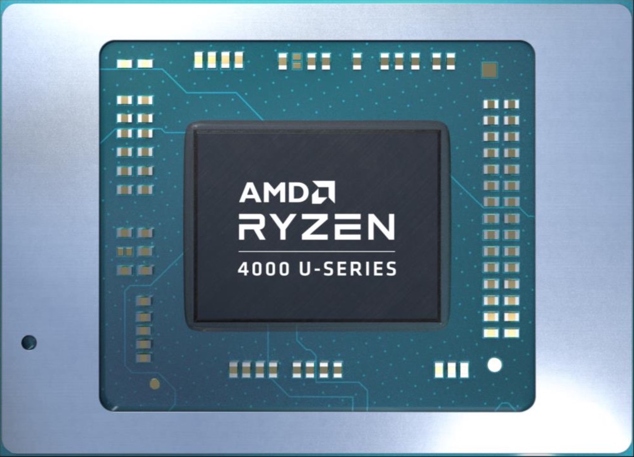
The AMD Ryzen 7 4980U is a Renoir family processor designed for certain Microsoft Surface systems. 4980U has eight Zen 2 cores clocked at 2.0 GHz (base clock speed) to 4.4 GHz (Boost) with thread-doubling SMT tech enabled for a total of 16 threads. The chip is manufactured on the modern 7 nm TSMC process and partly thanks to that AMD promises a 2x improvement in performance-per-Watt over Ryzen 3000 series mobile CPUs.
Architecture
The Zen 2 microarchitecture has brought a sizeable per-thread performance boost compared to the outgoing Zen+ parts. Renoir product family is also the first to introduce 8-core ULV processors to laptop market, keeping power consumption within reasonable limits. This AMD processor family is very impressive from most perspectives. One of the disatvantages to keep in mind is the lack of PCI-Express 4 support, meaning these blazing-fast NVMe SSDs will be limited to 3.9 GB/s tops.
Ryzen 7 4980U is designed to work with quad-channel LPDDR4 memory at up to 4,267 MHz. 8 MB of Level 3 are present in this chip. The Ryzen 7 gets soldered straight to the motherboard (FP6 socket) and is thus not user-replaceable. Please go to our Renoir hub page for more information on the product family.
Performance
The 4980U is the fastest U-class Ryzen 4000 series chip. As such, its clock speeds are 200 MHz higher (both the base one and Boost one) than what the Ryzen 7 4800U has.
It is thus hardly surprising that the average 4980U in our database is in the same league as the Ryzen 7 5800U and also the Core i7-1260P, as far as multi-thread benchmark scores are concerned.
Graphics
In addition to its eight CPU cores, the Ryzen 7 also features the Radeon RX Vega 8 graphics adapter with 8 CUs (= 512 shaders) at up to 1,950 MHz. This iGPU is compatible with FreeSync and DirectX 12 and is able to HW-decode AVC, HEVC, VP9-encoded videos (no AV1 support here). Vega 8 is capable of outputting UHD 2160p60 video signal to several monitors and, similar to Intel's Iris Xe (80 EUs), is good enough for a bit of light gaming on the go, provided one is content with sub-1080p resolutions and low/medium quailty presets.
Power consumption
The APU has a default TDP, also known as the long-term power limit, of 15 W; much like it is with other U-class Ryzen 4000 chips, AMD is fine with laptop makers (Microsoft, in this case) changing that value to anything between 10 W and 25 W.
The 7 nm TSMC process this Ryzen 7 is built with makes for above average, as of mid 2022, energy efficiency.
Intel Celeron J4025
► remove from comparison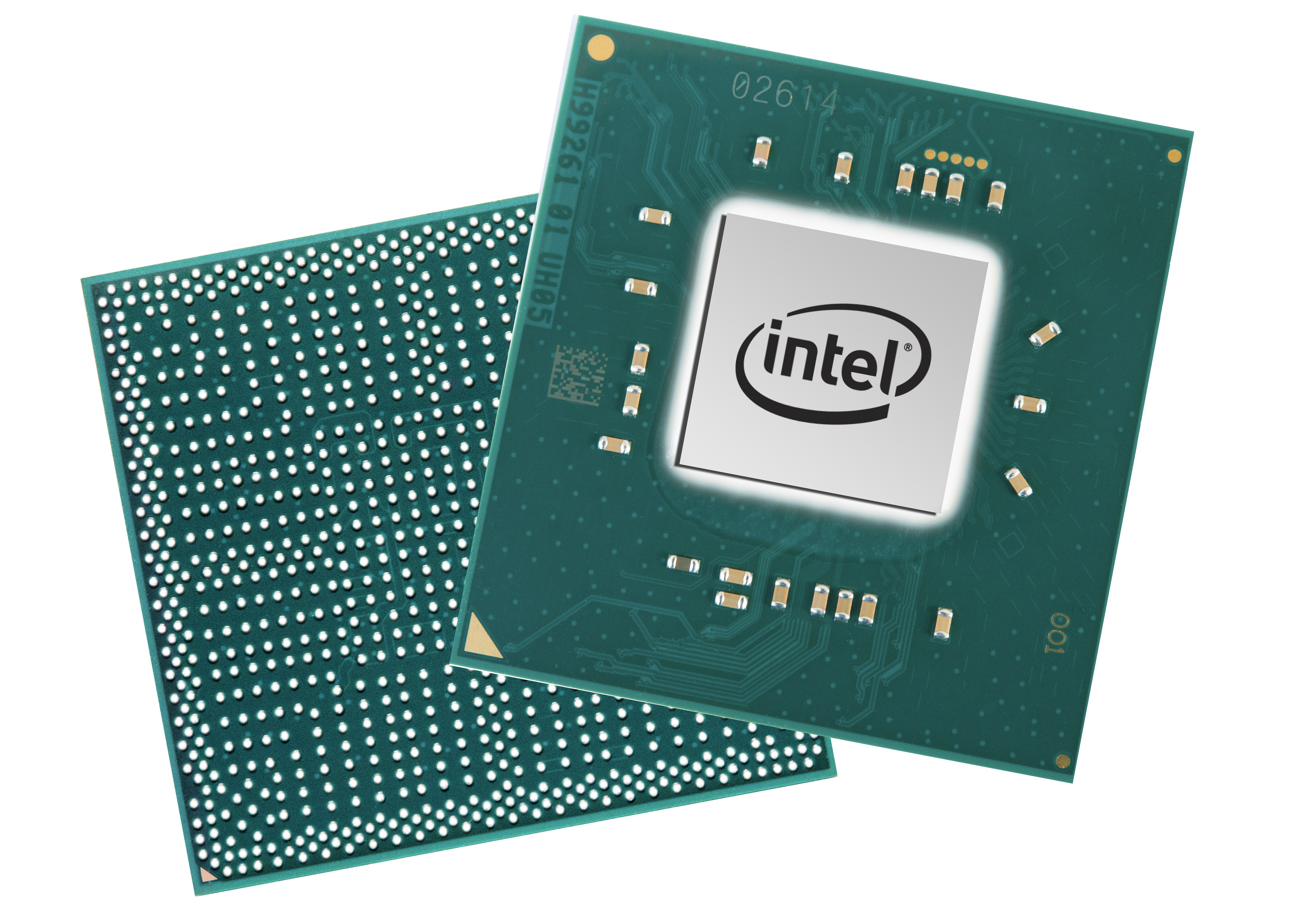
The Intel Celeron J4025 is an energy-efficient, dual-core processor (SoC) of the Gemini Lake Refresh product family; as such, it is designed for use in mini-PCs of the most affordable flavor. The Celeron was launched in Q4 2019. Its CPU cores run at 2 GHz to 2.9 GHz (single core boost). Other key specs include a DDR4/LPDDR4 memory controller (up to 2,400 MHz and up to 8 GB, with independent reports claiming as much as 32 GB will work just fine) and the integrated UHD Graphics 600 graphics adapter.
Architecture
Just like Apollo Lake family products, the ever-popular N3350 included, Celeron J4025 is manufactured by Intel on a 14 nm process. What makes these newer Celerons different are the slightly improved processor cores with double the L2 cache and also, somewhat counterintuitively, their smaller chip area.
The Goldmont Plus microarchitecture is familiar to us from Gemini Lake processors like the N4000. A moderately large 4 MB L2 cache features prominently on the rather short list of Goldmont Plus' strong sides, allowing for a marginal increase in performance-per-MHz figures compared to Goldmont. Still, Gemini Lake Refresh processors are a clear step-down from the Core i3/i5/i7/i9 series processors, both in performance and in features.
J4025 has six PCI-Express 2.0 lanes at its disposal. While very few J4025-based SBCs, nettops and laptops feature an NVMe M.2 slot, you can use an NVMe SSD as a boot drive with this processor (read/write rates will be limited to 2 GB/s though). Furthermore, partial Wi-Fi 5 support is built into the CPU. The Celeron also supports up to eight USB 3.0 ports and two SATA III storage devices.
Please note this is not a user-replaceable CPU. They solder it straight on to the motherboard for good (FCBGA1090 socket interface).
Performance
The Celeron J4025 is positioned in the lower entry level and only slightly faster than the mobile Celeron N4020. Therefore, it is best suited for basic tasks like word processing and web browsing with just two or three tabs open.
Graphics
The UHD Graphics 600 is based on Intel's Generation 9 architecture, much like HD Graphics 520 or UHD Graphics 615 or so many other widespread Intel iGPUs.
Just like HD Graphics 500, the UHD Graphics 600 supports DX 12 and has 12 EUs clocked at up to 650 MHz. The Iris Plus G7 iGPU that certain 10th Gen Ice Lake processors have packs 64 EUs, for reference. As a low-end solution, UHD Graphics 600 will let you play some seriously old titles, but that's about it.
Perhaps more importantly, this graphics solution will let you run up to 3 monitors with resolutions as high as 4096x2160@60. Furthermore, it will have no trouble HW-decoding AVC, HEVC and VP9 videos. The newer AV1 codec will be decoded via software, with the limited CPU horsepower imposing a hard limit on the video resolution that can be played back without stuttering. 1080p60 YouTube videos are out of reach while 720p25 videos run fine, to give you an example.
Power Consumption
As a J-series CPU, the TDP is rated at 10 Watts and therefore 4 W higher than the mobile N4020.
| Model | AMD Ryzen 7 4980U | Intel Celeron J4025 | ||||||||||||||||||||||||||||||||||||||||||||||||||||
| Series | AMD Renoir (Ryzen 4000 APU) | Intel Gemini Lake | ||||||||||||||||||||||||||||||||||||||||||||||||||||
| Codename | Renoir-U (Zen 2) | Gemini Lake Refresh | ||||||||||||||||||||||||||||||||||||||||||||||||||||
| Series: Gemini Lake Gemini Lake Refresh |
|
| ||||||||||||||||||||||||||||||||||||||||||||||||||||
| Clock | 2000 - 4400 MHz | 2000 - 2900 MHz | ||||||||||||||||||||||||||||||||||||||||||||||||||||
| L1 Cache | 512 KB | |||||||||||||||||||||||||||||||||||||||||||||||||||||
| L2 Cache | 4 MB | 4 MB | ||||||||||||||||||||||||||||||||||||||||||||||||||||
| L3 Cache | 8 MB | |||||||||||||||||||||||||||||||||||||||||||||||||||||
| Cores / Threads | 8 / 16 | 2 / 2 | ||||||||||||||||||||||||||||||||||||||||||||||||||||
| TDP | 15 Watt | 10 Watt | ||||||||||||||||||||||||||||||||||||||||||||||||||||
| Technology | 7 nm | 14 nm | ||||||||||||||||||||||||||||||||||||||||||||||||||||
| max. Temp. | 105 °C | 105 °C | ||||||||||||||||||||||||||||||||||||||||||||||||||||
| Socket | FP6 | FCBGA1090 | ||||||||||||||||||||||||||||||||||||||||||||||||||||
| Features | LPDDR4-4266 RAM, PCIe 3, MMX, SSE, SSE2, SSE3, SSSE3, SSE4A, SSE4.1, SSE4.2, AVX, AVX2, BMI2, ABM, FMA, ADX, SMEP, SMAP, SMT, CPB, AES-NI, RDRAND, RDSEED, SHA | Intel UHD Graphics 600 (12 EUs, 250 - 700 MHz), Quick Sync, AES-NI, max. 8 GB Dual-Channel DDR4/LPDDR4-2400 | ||||||||||||||||||||||||||||||||||||||||||||||||||||
| iGPU | AMD Radeon RX Vega 8 (Ryzen 4000/5000) ( - 1950 MHz) | Intel UHD Graphics 600 (250 - 700 MHz) | ||||||||||||||||||||||||||||||||||||||||||||||||||||
| Architecture | x86 | x86 | ||||||||||||||||||||||||||||||||||||||||||||||||||||
| Announced | ||||||||||||||||||||||||||||||||||||||||||||||||||||||
| Manufacturer | www.amd.com | ark.intel.com |

