 Deutsch
 English
 Español
 Français
 Italiano
 Nederlands
 Polski
 Português
 Русский
 Türkçe
 Svenska
 Chinese
 Magyar
AMD Ryzen 5 7600 vs AMD Ryzen 5 PRO 7540U vs AMD Ryzen Z1
AMD Ryzen 5 7600
► remove from comparison
The AMD Ryzen 5 7600 is a fast mid-range desktop processor of the Raphael series. It offers 6 cores based on the Zen 4 architecture that supports hyperthreading (12 threads). The cores clock from 3.8 (base) up to 5.1 GHz (single core boost).
The Raphael series still uses a chiplet design with two CCD-clusters (each with 8 possible cores) in 5nm and an IO-die (including the memory controller and the Radeon Graphics iGPU) in 6nm.
The R5 7600X is rated at 65 Watt TDP.
AMD Ryzen 5 PRO 7540U
► remove from comparison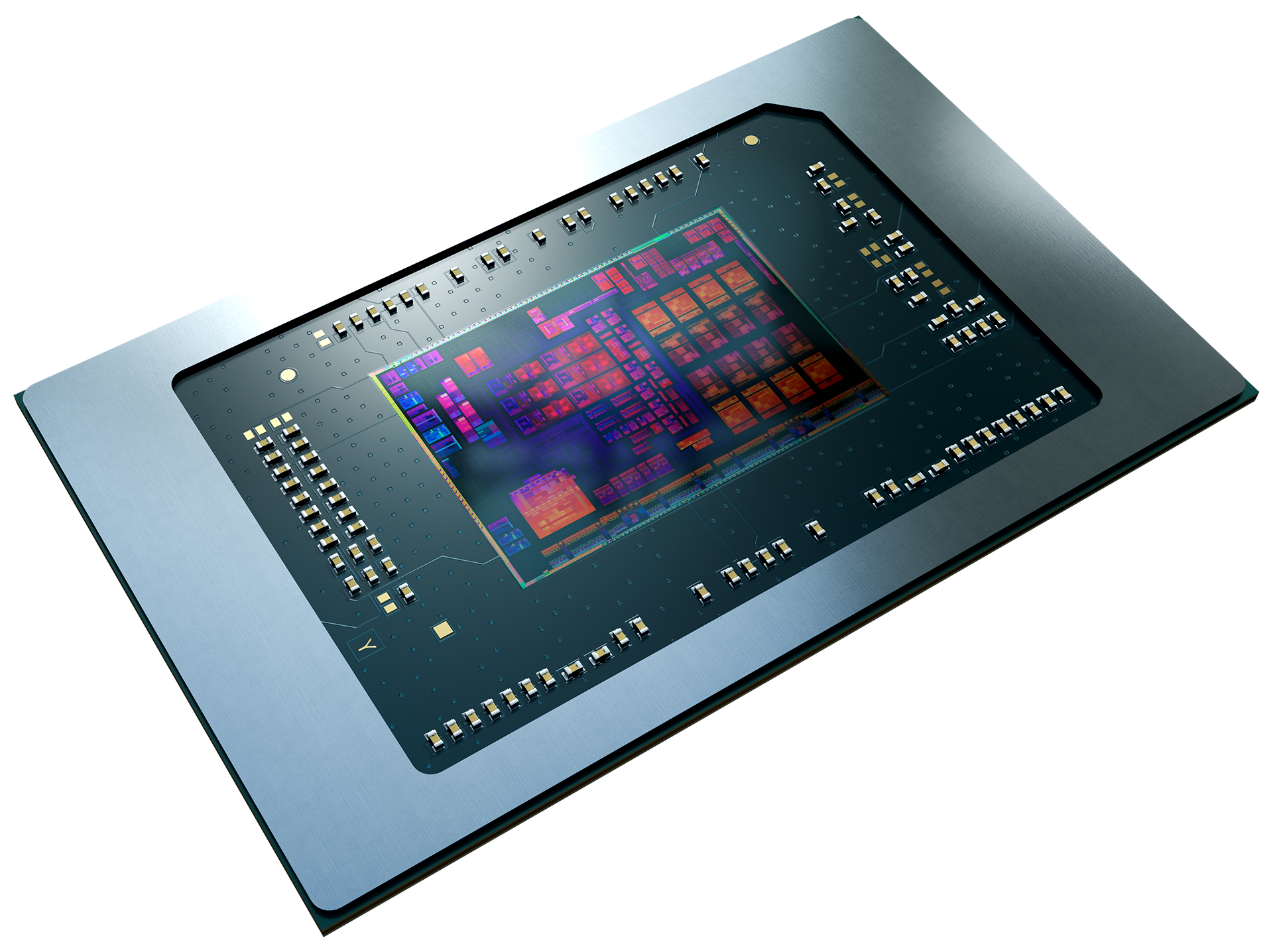
The AMD Ryzen 5 PRO 7540U is a fast mid-range laptop processor of the Phoenix series. It offers 6 cores (hexa core) based on the Zen 4 architecture that supports hyperthreading (12 threads). The cores clock from 3.2 (base) up to 4.9 GHz (single core boost). The processor includes 6 MB L2 cache and 16 MB L3 cache.
Compared to the consumer Ryzen 5 7540U, the PRO models offer additional security, manageability, and reliability features designed for professional users and workstation environments.
Thanks to the new Zen 4 architecture and higher clock speeds, the R5 PRO 7540U is clearly faster than the old Ryzen 5 6600U (Zen 3, 6 cores, 4.5 GHz). Compared to the similar PRO 7640U, the 7540U offers a lower base clock and a slower iGPU.
The chip integrates a modern and fasts RDNA 3 graphics card (iGPU) called Radeon 740M with 4 of the 12 CUs and 2.5 GHz clock speed. Furthermore, the Phoenix series include a video engine with AV1 de- and encoding, a new Xilinx FPGA based XDNA AI accelerator (Ryzen AI) that should be faster than the AI engine in the Apple M2 SOC and a dual-channel DDR5-5600 / LPDDR5x-7500 memory controller (with ECC support). The connectivity features includes 2 possible USB 4 (40 Gbps) ports and 20 PCIe 4.0 lanes for a GPU and SSDs.
The Phoenix series uses a single monolithic design (unlike the chiplet design of the 7045HX series) and is manufactured in the modern 4nm process at TSMC. The TDP can be configured between 35 and 45 Watt.
AMD Ryzen Z1
► remove from comparisonThe AMD Ryzen Z1 is a fast mid-range laptop processor of the Phoenix series. It offers 6 cores (hexa core) based on the Zen 4 architecture that supports SMT (hyperthreading, 12 threads). The cores clock from 3.2 (base) up to 4.9 GHz (single core boost). The processor includes 6 MB L2 cache and 16 MB L3 cache.
Thanks to the new Zen 4 architecture and higher clock speeds, the Ryzen Z1 is clearly faster than the old Ryzen 5 6600U (Zen 3, 6 cores, 4.5 GHz). Compared to the similar Ryzen 5 7540U, the Z1 offers a higher boost clock, lower (optional TDP) and no AI accelerator.
The chip integrates a modern and fasts RDNA 3 graphics card (iGPU) called Radeon 740M with 4 of the 12 CUs and 2.5 GHz clock speed. Furthermore, the Phoenix series include a video engine with AV1 de- and encoding and a dual-channel DDR5-5600 / LPDDR5x-7500 memory controller (with ECC support). The connectivity features includes 2 possible USB 4 (40 Gbps) ports and 20 PCIe 4.0 lanes for a GPU and SSDs.
The Phoenix series uses a single monolithic design (unlike the chiplet design of the 7045HX series) and is manufactured in the modern 4nm process at TSMC. The TDP can be configured between 35 and 45 Watt.
| Model | AMD Ryzen 5 7600 | AMD Ryzen 5 PRO 7540U | AMD Ryzen Z1 | ||||||||||||||||||||||||||||||||||||||||||||||||||||||||||||||||||||||||||||||||
| Series | AMD Raphael (Zen 4, Ryzen 7000) | AMD Phoenix (Zen 4, Ryzen 7040) | AMD Phoenix (Zen 4, Ryzen 7040) | ||||||||||||||||||||||||||||||||||||||||||||||||||||||||||||||||||||||||||||||||
| Codename | Raphael (Zen4) | Phoenix (Zen4) | Phoenix (Zen4) | ||||||||||||||||||||||||||||||||||||||||||||||||||||||||||||||||||||||||||||||||
| Series: Phoenix (Zen 4, Ryzen 7040) Phoenix (Zen4) |
|
|
| ||||||||||||||||||||||||||||||||||||||||||||||||||||||||||||||||||||||||||||||||
| Clock | 3800 - 5100 MHz | 3200 - 4900 MHz | 3200 - 4900 MHz | ||||||||||||||||||||||||||||||||||||||||||||||||||||||||||||||||||||||||||||||||
| L1 Cache | 384 KB | 384 KB | 384 KB | ||||||||||||||||||||||||||||||||||||||||||||||||||||||||||||||||||||||||||||||||
| L2 Cache | 6 MB | 6 MB | 6 MB | ||||||||||||||||||||||||||||||||||||||||||||||||||||||||||||||||||||||||||||||||
| L3 Cache | 32 MB | 16 MB | 16 MB | ||||||||||||||||||||||||||||||||||||||||||||||||||||||||||||||||||||||||||||||||
| Cores / Threads | 6 / 12 | 6 / 12 6 x 4.9 GHz AMD Zen 4 | 6 / 12 | ||||||||||||||||||||||||||||||||||||||||||||||||||||||||||||||||||||||||||||||||
| TDP | 65 Watt | 15 Watt | 30 Watt | ||||||||||||||||||||||||||||||||||||||||||||||||||||||||||||||||||||||||||||||||
| Transistors | CCD: 6,5 Mrd + IOD: 3,4 Mrd Million | ||||||||||||||||||||||||||||||||||||||||||||||||||||||||||||||||||||||||||||||||||
| Technology | 5 nm, 0.650 - 1.475V | 4 nm | 4 nm | ||||||||||||||||||||||||||||||||||||||||||||||||||||||||||||||||||||||||||||||||
| Die Size | 1x 70 (CCD) mm2 + 122 (I/O) mm2 | 178 mm2 | 178 mm2 | ||||||||||||||||||||||||||||||||||||||||||||||||||||||||||||||||||||||||||||||||
| max. Temp. | 95 °C | 100 °C | 100 °C | ||||||||||||||||||||||||||||||||||||||||||||||||||||||||||||||||||||||||||||||||
| Socket | AM5 (LGA 1718) | ||||||||||||||||||||||||||||||||||||||||||||||||||||||||||||||||||||||||||||||||||
| Features | MMX(+), SSE, SSE2, SSE3, SSSE3, SSE4.1, SSE4.2, SSE4A, x86-64, AMD-V, AES, AVX, AVX2, AVX512F, FMA3, SHA, Precision Boost 2 | ||||||||||||||||||||||||||||||||||||||||||||||||||||||||||||||||||||||||||||||||||
| iGPU | AMD Radeon Graphics (Ryzen 7000) (400 - 2200 MHz) | AMD Radeon 740M ( - 2500 MHz) | AMD Radeon 740M | ||||||||||||||||||||||||||||||||||||||||||||||||||||||||||||||||||||||||||||||||
| Architecture | x86 | x86 | x86 | ||||||||||||||||||||||||||||||||||||||||||||||||||||||||||||||||||||||||||||||||
| Announced | |||||||||||||||||||||||||||||||||||||||||||||||||||||||||||||||||||||||||||||||||||
| Manufacturer | www.amd.com | www.amd.com | www.amd.com |
