 Deutsch
 English
 Español
 Français
 Italiano
 Nederlands
 Polski
 Português
 Русский
 Türkçe
 Svenska
 Chinese
 Magyar
AMD Ryzen 5 7520U vs Intel Pentium 8500
AMD Ryzen 5 7520U
► remove from comparison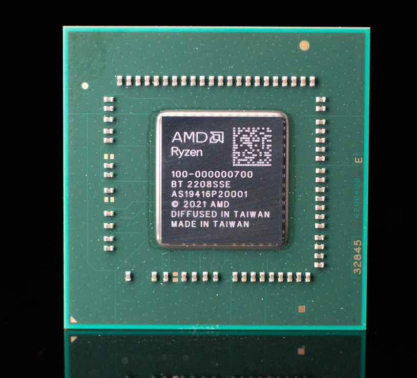
The AMD Ryzen 5 7520U is a mobile processor for cheap laptops of the Mendocino series. It integrates four older Zen 2 cores (similar to the Ryzen 4000 series like the Ryzen 3 4300U). The CPU cores clock from 2.8 GHz (base) to 4.3 GHz (single core Turbo) and can use 4 MB L3 cache. Thanks to SMT/Hyperthreading, the CPU can work on 8 threads simultaneously. The integrated memory controller only supports fast LPDDR5 memory (5500 MHz max.).
The integrated graphics adapter (Radeon 610M iGPU) uses the modern RDNA 2 architecture, but only 2 CUs (128 shaders) and clocks with up to 1.9 GHz.
Performance
The average 7520U in our extensive database is in the same league as the Core i7-1185G7, as far as multi-thread benchmark scores are concerned. This is a so-so result and indicative of a lower mid-range chip, as of Q3 2023.
Your mileage may vary depending on how high the CPU power limits are and how competent the cooling solution of your system is.
Mendocino series chips are produced on a relatively modern 6nm FinFET process at TSMC and should offer a good power efficiency. The R5 7520U is rated at 8-15 W TDP and therefore well suited for thin and light laptops.
Intel Pentium 8500
► remove from comparisonThe Intel Pentium 8500 is an entry-level low-power mobile CPU for thin and light laptops based on the Alder Lake architecture. It was announced in early 2022 and offers one performance core (P-cores, Golden Cove architecture) and 4 efficient cores (E-cores, Gracemont architecture). The P-cores support Hyper-Threading leading to 6 supported threads when combined with the E-cores. The clock rate ranges from 1 to 4.4 GHz on the performance cluster and 0.7 to 3.3 GHz on the efficient cluster. The performance of the E-cores should be similar to old Skylake cores (compare to the Core i7-6700HQ). All cores can use up to 8 MB L3-cache. Compared to the faster Core i3-1210U, the Pentium offers one less P-core.
Performance
While we have not tested a single system built around the 8500 as of August 2023, it's safe to expect the chip to be about 20% slower than the i3-1215U, as far as multi-thread performance is concerned. Which is pretty terrible as of Q3 2023.
Your mileage may vary depending on how high the CPU power limits are and how competent the cooling solution of your system is.
Features
The integrated memory controller supports various memory types up to DDR5-4800, DDR4-3200, LPDDR5-5200, and LPDDR4x-4267. The Thread Director (in hardware) can support the operating system to decide which thread to use on the performance or efficient cores for the best performance. For AI tasks, the CPU also integrates GNA 3.0 and DL Boost (via AVX2). Quick Sync in version 8 is the same as in the Rocket Lake CPUs and supports MPEG-2, AVC, VC-1 decode, JPEG, VP8 decode, VP9, HEVC, and AV1 decode in hardware. The CPU only supports PCIe 4.0 (x8 for a GPU and two x4 for SSDs).
The integrated graphics adapter is based on the Xe-architecture and offers 48 of the 96 EUs (Execution Units) operating at up to 0.8 GHz.
Power consumption
This Pentium has a Base power consumption of 9 W, with 29 W being its maximum Intel-recommended Turbo power consumption. TDP values this low allow for passively cooled laptops, tablets, mini-PCs as long as performance is not a priority.
The CPU is made with Intel's 3rd generation 10 nm process marketed as Intel 7 for decent, as of early 2023, energy efficiency.
| Model | AMD Ryzen 5 7520U | Intel Pentium 8500 | ||||||||||||||||||||||||||||||||||||||||||||||||||||||||||||||||
| Series | AMD Mendocino (Zen 2, Ryzen 7020) | Intel Alder Lake-M | ||||||||||||||||||||||||||||||||||||||||||||||||||||||||||||||||
| Codename | Mendocino-U (Zen 2) | Alder Lake-U | ||||||||||||||||||||||||||||||||||||||||||||||||||||||||||||||||
| Series: Alder Lake-M Alder Lake-U |
|
| ||||||||||||||||||||||||||||||||||||||||||||||||||||||||||||||||
| Clock | 2800 - 4300 MHz | 700 - 4400 MHz | ||||||||||||||||||||||||||||||||||||||||||||||||||||||||||||||||
| L1 Cache | 256 KB | 464 KB | ||||||||||||||||||||||||||||||||||||||||||||||||||||||||||||||||
| L2 Cache | 2 MB | 3.5 MB | ||||||||||||||||||||||||||||||||||||||||||||||||||||||||||||||||
| L3 Cache | 4 MB | 8 MB | ||||||||||||||||||||||||||||||||||||||||||||||||||||||||||||||||
| Cores / Threads | 4 / 8 | 5 / 6 | ||||||||||||||||||||||||||||||||||||||||||||||||||||||||||||||||
| TDP | 15 Watt | 9 Watt | ||||||||||||||||||||||||||||||||||||||||||||||||||||||||||||||||
| Technology | 6 nm | 10 nm | ||||||||||||||||||||||||||||||||||||||||||||||||||||||||||||||||
| Features | LPDDR5-5500 RAM, PCIe 3, MMX (+), SSE, SSE2, SSE3, SSSE3, SSE4.1, SSE4.2, SSE4A, AES, AVX, AVX2, FMA3, SHA | LPDDR4x-4266/LPDDR5-5200 RAM, PCIe 4, Thr. Director, DL Boost, GNA, MMX, SSE, SSE2, SSE3, SSSE3, SSE4.1, SSE4.2, AES, AVX, AVX2, FMA3, SHA | ||||||||||||||||||||||||||||||||||||||||||||||||||||||||||||||||
| iGPU | AMD Radeon 610M ( - 1900 MHz) | Intel UHD Graphics Xe G4 48EUs ( - 800 MHz) | ||||||||||||||||||||||||||||||||||||||||||||||||||||||||||||||||
| Architecture | x86 | x86 | ||||||||||||||||||||||||||||||||||||||||||||||||||||||||||||||||
| Announced | ||||||||||||||||||||||||||||||||||||||||||||||||||||||||||||||||||
| Manufacturer | www.amd.com | ark.intel.com | ||||||||||||||||||||||||||||||||||||||||||||||||||||||||||||||||
| max. Temp. | 100 °C | |||||||||||||||||||||||||||||||||||||||||||||||||||||||||||||||||
| Socket | BGA1744 |
