 Deutsch
 English
 Español
 Français
 Italiano
 Nederlands
 Polski
 Português
 Русский
 Türkçe
 Svenska
 Chinese
 Magyar
Intel Pentium Silver N6000 vs AMD Ryzen 5 7540U vs Intel Celeron N5100
Intel Pentium Silver N6000
► remove from comparisonThe Intel Pentium Silver N6000 is a quad-core SoC of the Jasper Lake series that is primarily intended for inexpensive notebooks and was announced in early 2021. The four Tremont CPU cores clock between 1.1 and 3.3 GHz (single core Burst) and offer no HyperThreading (SMT). The N6000 uses 1.5 MB L2 and 4 MB L3 cache. The chip is manufactured on the first-gen 10 nm Intel process, the same process as Ice Lake.
Architecture
The processor architecture is called Tremont and a complete redesign compared to the old Golmont Plus cores in the predecessor. According to Intel, the single thread performance of a core could be improved by 30% on average (10 - 80% in all tests of SPECint and SPECfp).
Features
In addition to the four CPU cores, the SoC integrates a 32 EU Intel UHD Graphics GPU clocked from 350 - 850 MHz and a dual-channel DDR4 / quad-channel LPDDR4x memory controller (up to 16 GB and 2933 MHz). The chip now also partly integrates Wi-Fi 6 (Gig+), 8 PCIe 3.0 lanes, 14 USB 2.0/ 3.2 ports and two SATA 6.0 ports. The package got bigger and measures 35 x 24 mm (compared to 25 x 24 mm for the N5030 e.g.). The SoC is directly soldered to the mainboard (BGA) and can't be easily replaced.
Performance
The average N6000 in our database proves to be an OK entry-level processor, as of late 2022, its multi-thread benchmark scores nearly matching those of the AMD Ryzen 3 3200U. Yes, the chip is a whole lot slower than the latest Ryzen 3 and Core i3 processors, but it will at least let you run your day-to-day apps without annoying slowdowns.
The Asus Vivobook 13 Slate is among the fastest systems built around the N6000 that we know of, thanks to the long-term CPU power limit of 10 W. It can be more than 20% faster in CPU-bound workloads than the slowest system featuring the same chip in our database, as of August 2023.
Power consumption
Like nearly all other N-class Intel processors, the Pentium N6000 has a default TDP of 6 W (also known as the long-term power limit). This is low and thus good enough for passively cooled tablets, laptops, mini-PCs.
The SoC is built with Intel's 2nd generation 10 nm process (not 10 nm SuperFin or Intel 7) for low, as of mid 2023, energy efficiency.
AMD Ryzen 5 7540U
► remove from comparison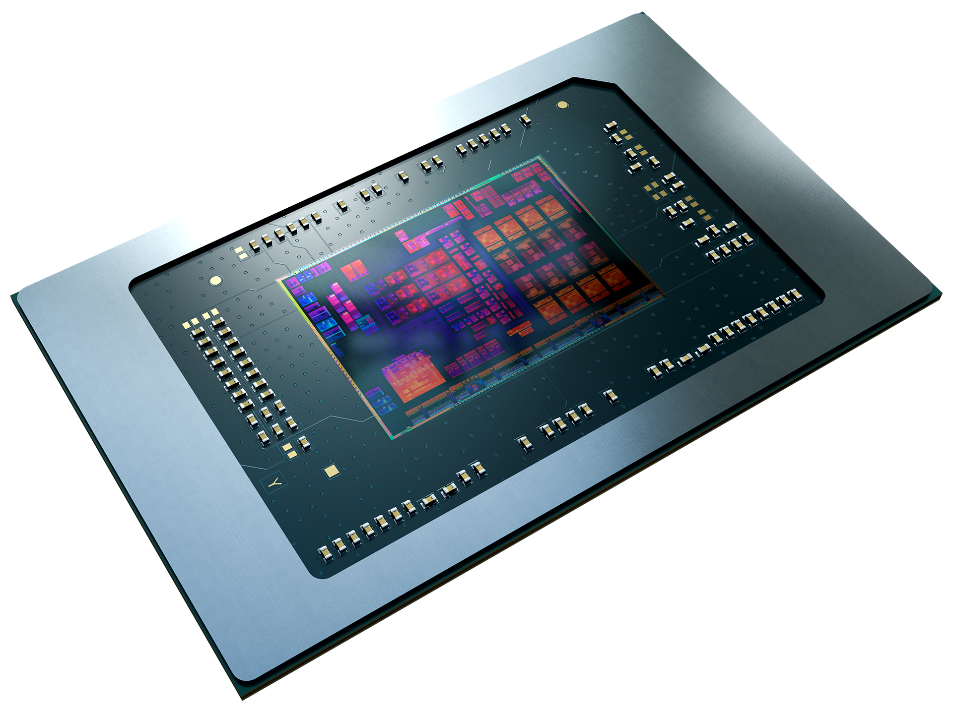
The AMD Ryzen 5 7540U is a fast mid-range laptop processor of the Phoenix series. It offers 6 cores (hexa core) based on the Zen 4 architecture that supports hyperthreading (12 threads). The cores clock from 3.2 (base) up to 4.9 GHz (single core boost). The processor includes 6 MB L2 cache and 16 MB L3 cache.
Thanks to the new Zen 4 architecture and higher clock speeds, the R5 7540U is clearly faster than the old Ryzen 5 6600U (Zen 3, 6 cores, 4.5 GHz). Compared to the similar 7640U, the 7540U offers a lower base clock and a slower iGPU.
The chip integrates a modern and fasts RDNA 3 graphics card (iGPU) called Radeon 740M with 4 of the 12 CUs and 2.5 GHz clock speed. Furthermore, the Phoenix series include a video engine with AV1 de- and encoding and a dual-channel DDR5-5600 / LPDDR5x-7500 memory controller (with ECC support). The new Xilinx FPGA based XDNA AI accelerator (Ryzen AI) is not included in the 7540U. The connectivity features includes 2 possible USB 4 (40 Gbps) ports and 20 PCIe 4.0 lanes for a GPU and SSDs.
The Phoenix series uses a single monolithic design (unlike the chiplet design of the 7045HX series) and is manufactured in the modern 4nm process at TSMC. The TDP can be configured between 15 and 30 Watt (28 Watt default).
Intel Celeron N5100
► remove from comparisonThe Intel Celeron N5100 is a quad-core SoC of the Jasper Lake series that is primarily intended for inexpensive notebooks and was announced in early 2021. The four Tremont CPU cores clock between 1.1 and 2.8 GHz (single core Burst) and offer no HyperThreading (SMT). The N5100 uses 1.5 MB L2 and 4 MB L3 cache. The chip is manufactured in 10nm at Intel (most likely in the same process as Ice Lake).
Architecture
The processor architecture is called Tremont and a complete redesign compared to the old Golmont Plus cores in the predecessor. According to Intel, the single thread performance of a core could be improved by 30% on average (10 - 80% in all tests of SPECint and SPECfp).
Features
In addition to the quad-core CPU block, the SoC integrates a 24 EU Intel UHD Graphics GPU clocked from 350 - 800 MHz and a LPDDR4(x) dual channel memory controller (up to 16 GB and 2933 MHz). The chip now also partly integrates Wi-Fi 6 (Gig+), 8 PCIe 3.0 lanes, 14 USB 2.0/ 3.2 ports and two SATA 6.0 ports. The package got bigger and measures 35 x 24 mm (compared to 25 x 24 mm for the N5030 e.g.). The SoC is directly soldered to the mainboard (BGA) and can't be easily replaced.
Performance
While we have not tested a single system powered by the N5100 as of August 2023, it's safe to expect the chip to be 10% to 20% slower than the N6000, as far as multi-thread performance is concerned. In other words, this is a fairly slow processor that is unlikely to make anybody happy.
Power Consumption
Like most other N-class Intel processors, this Celeron has a 6 W default TDP (also known as the long-term power limit). This is rather low; a small metal plate is all it takes to dissipate heat generated by such a CPU.
The Celeron N5100 is manufactured on Intel's first-generation or second-generation [no exact data available] 10 nm process for average, as of early 2023, energy efficiency.
| Model | Intel Pentium Silver N6000 | AMD Ryzen 5 7540U | Intel Celeron N5100 | ||||||||||||||||||||||||||||||||||||||||||||||||||||||||||||||||||||||||||||||||
| Series | Intel Jasper Lake | AMD Phoenix (Zen 4, Ryzen 7040) | Intel Jasper Lake | ||||||||||||||||||||||||||||||||||||||||||||||||||||||||||||||||||||||||||||||||
| Codename | Jasper Lake | Phoenix (Zen4) | Jasper Lake | ||||||||||||||||||||||||||||||||||||||||||||||||||||||||||||||||||||||||||||||||
| Series: Jasper Lake Jasper Lake |
|
|
| ||||||||||||||||||||||||||||||||||||||||||||||||||||||||||||||||||||||||||||||||
| Clock | 1100 - 3300 MHz | 3200 - 4900 MHz | 1100 - 2800 MHz | ||||||||||||||||||||||||||||||||||||||||||||||||||||||||||||||||||||||||||||||||
| L2 Cache | 1.5 MB | 6 MB | 1.5 MB | ||||||||||||||||||||||||||||||||||||||||||||||||||||||||||||||||||||||||||||||||
| L3 Cache | 4 MB | 16 MB | 4 MB | ||||||||||||||||||||||||||||||||||||||||||||||||||||||||||||||||||||||||||||||||
| Cores / Threads | 4 / 4 | 6 / 12 6 x 4.9 GHz AMD Zen 4 | 4 / 4 | ||||||||||||||||||||||||||||||||||||||||||||||||||||||||||||||||||||||||||||||||
| TDP | 6 Watt | 28 Watt | 6 Watt | ||||||||||||||||||||||||||||||||||||||||||||||||||||||||||||||||||||||||||||||||
| Technology | 10 nm | 4 nm | 10 nm | ||||||||||||||||||||||||||||||||||||||||||||||||||||||||||||||||||||||||||||||||
| max. Temp. | 105 °C | 100 °C | 105 °C | ||||||||||||||||||||||||||||||||||||||||||||||||||||||||||||||||||||||||||||||||
| Socket | BGA1338 | BGA1338 | |||||||||||||||||||||||||||||||||||||||||||||||||||||||||||||||||||||||||||||||||
| Features | DDR4-2933/LPDDR4x-2933 RAM, PCIe 3 x 8, GNA, MMX, SSE, SSE2, SSE3, SSSE3, SSE4.1, SSE4.2, SMEP, SMAP, EIST, TM1, TM2, Turbo, SST, AES-NI, RDRAND, RDSEED, SHA | DDR4-2933/LPDDR4x-2933 RAM, PCIe 3, GNA, MMX, SSE, SSE2, SSE3, SSSE3, SSE4.1, SSE4.2, VMX, SMEP, SMAP, EIST, TM1, TM2, Turbo, AES-NI, RDRAND, RDSEED, SHA | |||||||||||||||||||||||||||||||||||||||||||||||||||||||||||||||||||||||||||||||||
| iGPU | Intel UHD Graphics (Jasper Lake 32 EU) (350 - 850 MHz) | AMD Radeon 740M ( - 2500 MHz) | Intel UHD Graphics (Jasper Lake 24 EU) (350 - 800 MHz) | ||||||||||||||||||||||||||||||||||||||||||||||||||||||||||||||||||||||||||||||||
| Architecture | x86 | x86 | x86 | ||||||||||||||||||||||||||||||||||||||||||||||||||||||||||||||||||||||||||||||||
| Announced | |||||||||||||||||||||||||||||||||||||||||||||||||||||||||||||||||||||||||||||||||||
| Manufacturer | ark.intel.com | www.amd.com | ark.intel.com | ||||||||||||||||||||||||||||||||||||||||||||||||||||||||||||||||||||||||||||||||
| L1 Cache | 384 KB | ||||||||||||||||||||||||||||||||||||||||||||||||||||||||||||||||||||||||||||||||||
| Die Size | 178 mm2 |

