 Deutsch
 English
 Español
 Français
 Italiano
 Nederlands
 Polski
 Português
 Русский
 Türkçe
 Svenska
 Chinese
 Magyar
Apple M1 Max vs Intel Core i7-5650U
Apple M1 Max
► remove from comparison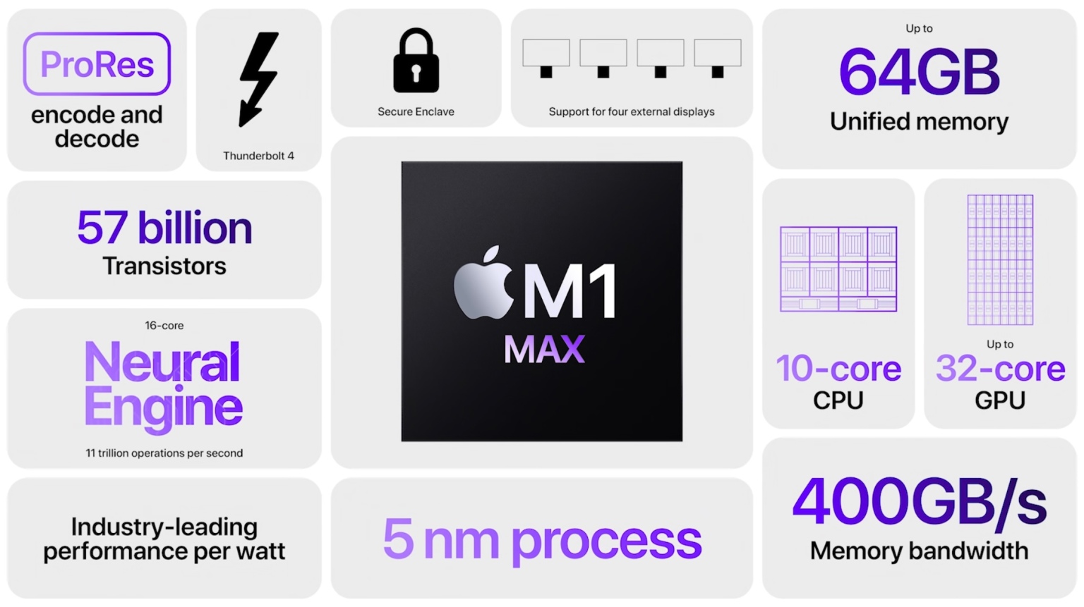
The Apple M1 Max is a System on a Chip (SoC) from Apple that is found in the late 2021 MacBook Pro 14 and 16-inch models. It offers all 10 cores available in the chip divided in eight performance cores (P-cores with 600 - 3220 MHz) and two power-efficiency cores (E-cores with 600 - 2064 MHz). There is no Turbo Boost for single cores or short burst periods. The cores are similar to the cores in the Apple M1.
The big cores (codename Firestorm) offer 192 KB instruction cache, 128 KB data cache, and 24 MB shared L2 cache (up from 12 MB in the M1). The four efficiency cores (codename Icestorm) are a lot smaller and offer only 128 KB instruction cache, 64 KB data cache, and 4 MB shared cache. CPU and GPU can both use the 48 MB SLC (System Level Cache). The efficiency cores (E cluster) clock with 600 - 2064 MHz, the performance cores (P cluster) with 600 - 3228 MHz.
The unified memory (32 or 64 GB LPDDR5-6400) next to the chip is connected by a 512 bit memory controller (200 GB/s bandwidth) and can be used by the GPU and CPU. This is the main difference to the M1 Pro and the CPU performance is quite similar.
The biggest difference to the M1 Pro is the bigger integrated GPU with 24 or 32 cores (up from 16).
Furthermore, the SoC integrates a fast 16 core neural engine, a secure enclave (e.g., for encryption), a unified memory architecture, Thunderbolt 4 controller, an ISP, and media de- and encoders (including two ProRes engines).
The M1 Pro is manufactured in 5 nm at TSMC and integrates 57 billion transistors. The peak power consumption of the chip was advertised around 30W for CPU intensive tasks.
Intel Core i7-5650U
► remove from comparisonThe Intel Core i7-5650U is an ULV (ultra low voltage) dual-core processor based on the Broadwell architecture, which has been launched in January 2015. In addition to two CPU cores with Hyper-Threading clocked at 2.2 - 3.2 GHz (2 Cores: 3.1 GHz), the chip also integrates an HD Graphics 6000 GPU and a dual-channel LPDDR3-1866/DDR3L-1600 memory controller. The Core i7 is manufactured in a 14 nm process with FinFET transistors.
Compared to the Core i7-5600U, the i7-5650U features a lower CPU base clock, but integrates a somewhat faster GPU.
Architecture
Broadwell represents the "Tick" in Intel's Tick-Tock model, which means a shrink of its predecessor Haswell. The new 14 nm manufacturing process with three-dimensional FinFET transistors allows not only improvements in energy efficiency, but also a significantly smaller die size fit for more compact packages and devices.
Further advantages result from the revised microarchitecture of Broadwell. Due to its improved branch prediction, bigger buffer sizes (1500 instead of 1000 entries in the L2 TLB) and other tweaks, the performance per clock has been increased by more than 5 percent over its predecessor. There are also some new instruction set extensions designed for cryptographic applications.
Performance
Thanks to its improved architecture, the Core i7-5650U is about 5 - 20 percent faster than the slightly lower clocked Core i7-4650U (Haswell, 15 W) and matches the Core i5-4288U (Haswell, 28 W). Thus, the CPU has sufficient power even for demanding applications and multitasking.
Graphics
The integrated HD Graphics 6000 offers 48 Execution Units (EUs) clocked at 300 - 1000 MHz. Similar to the CPU core, the GPU architecture (Intel Gen 8) has been thoroughly revised for improved performance-per-clock. In addition, the GPU benefits from faster memory speeds up to LPDDR3-1866 (Haswell: DDR3-1600). We expect the HD Graphics 6000 to be significantly faster than the former HD Graphics 5000 (40 EUs), part of the Haswell generation. Nevertheless, demanding games as of 2015 should be playable only in low or medium settings.
Broadwell is the first Intel chip to fully support DirectX 11.2 as well as OpenCL 1.3/2.0 and OpenGL 4.3. Video will output natively via DisplayPort 1.2 or HDMI 1.4a. However, the new HDMI 2.0 standard is not officially supported.
Power Consumption
The i7-5650U is rated at a TDP of 15 W (cTDP Down: 9.5 W) including the graphics card, memory controller, VRMs and the integrated chipset. Therefore, the CPU is suited even for small ultrabooks 11-inches and greater.
| Model | Apple M1 Max | Intel Core i7-5650U | ||||||||||||||||||||||||||||||||||||||||||||||||||||
| Series | Apple Apple M-Series | Intel Core i7 | ||||||||||||||||||||||||||||||||||||||||||||||||||||
| Series: Core i7 Broadwell |
|
| ||||||||||||||||||||||||||||||||||||||||||||||||||||
| Clock | 2060 - 3220 MHz | 2200 - 3200 MHz | ||||||||||||||||||||||||||||||||||||||||||||||||||||
| L1 Cache | 2.9 MB | 128 KB | ||||||||||||||||||||||||||||||||||||||||||||||||||||
| L2 Cache | 28 MB | 512 KB | ||||||||||||||||||||||||||||||||||||||||||||||||||||
| L3 Cache | 48 MB | 4 MB | ||||||||||||||||||||||||||||||||||||||||||||||||||||
| Cores / Threads | 10 / 10 | 2 / 4 | ||||||||||||||||||||||||||||||||||||||||||||||||||||
| Transistors | 57000 Million | 1900 Million | ||||||||||||||||||||||||||||||||||||||||||||||||||||
| Technology | 5 nm | 14 nm | ||||||||||||||||||||||||||||||||||||||||||||||||||||
| Features | ARMv8 Instruction Set | LPDDR3-1866/DDR3L-1600 Memory Controller, HyperThreading, AVX, AVX2, Quick Sync, Virtualization, vPro, AES-NI | ||||||||||||||||||||||||||||||||||||||||||||||||||||
| iGPU | Apple M1 Max 32-Core GPU | Intel HD Graphics 6000 (300 - 1000 MHz) | ||||||||||||||||||||||||||||||||||||||||||||||||||||
| Architecture | ARM | x86 | ||||||||||||||||||||||||||||||||||||||||||||||||||||
| Announced | ||||||||||||||||||||||||||||||||||||||||||||||||||||||
| Codename | Broadwell | |||||||||||||||||||||||||||||||||||||||||||||||||||||
| TDP | 15 Watt | |||||||||||||||||||||||||||||||||||||||||||||||||||||
| Die Size | 133 mm2 | |||||||||||||||||||||||||||||||||||||||||||||||||||||
| max. Temp. | 105 °C | |||||||||||||||||||||||||||||||||||||||||||||||||||||
| Socket | BGA | |||||||||||||||||||||||||||||||||||||||||||||||||||||
| $426 U.S. | ||||||||||||||||||||||||||||||||||||||||||||||||||||||
| Manufacturer | ark.intel.com |
