 Deutsch
 English
 Español
 Français
 Italiano
 Nederlands
 Polski
 Português
 Русский
 Türkçe
 Svenska
 Chinese
 Magyar
Intel Celeron N5100 vs Intel Core i3-N300
Intel Celeron N5100
► remove from comparisonThe Intel Celeron N5100 is a quad-core SoC of the Jasper Lake series that is primarily intended for inexpensive notebooks and was announced in early 2021. The four Tremont CPU cores clock between 1.1 and 2.8 GHz (single core Burst) and offer no HyperThreading (SMT). The N5100 uses 1.5 MB L2 and 4 MB L3 cache. The chip is manufactured in 10nm at Intel (most likely in the same process as Ice Lake).
Architecture
The processor architecture is called Tremont and a complete redesign compared to the old Golmont Plus cores in the predecessor. According to Intel, the single thread performance of a core could be improved by 30% on average (10 - 80% in all tests of SPECint and SPECfp).
Features
In addition to the quad-core CPU block, the SoC integrates a 24 EU Intel UHD Graphics GPU clocked from 350 - 800 MHz and a LPDDR4(x) dual channel memory controller (up to 16 GB and 2933 MHz). The chip now also partly integrates Wi-Fi 6 (Gig+), 8 PCIe 3.0 lanes, 14 USB 2.0/ 3.2 ports and two SATA 6.0 ports. The package got bigger and measures 35 x 24 mm (compared to 25 x 24 mm for the N5030 e.g.). The SoC is directly soldered to the mainboard (BGA) and can't be easily replaced.
Performance
While we have not tested a single system powered by the N5100 as of August 2023, it's safe to expect the chip to be 10% to 20% slower than the N6000, as far as multi-thread performance is concerned. In other words, this is a fairly slow processor that is unlikely to make anybody happy.
Power Consumption
Like most other N-class Intel processors, this Celeron has a 6 W default TDP (also known as the long-term power limit). This is rather low; a small metal plate is all it takes to dissipate heat generated by such a CPU.
The Celeron N5100 is manufactured on Intel's first-generation or second-generation [no exact data available] 10 nm process for average, as of early 2023, energy efficiency.
Intel Core i3-N300
► remove from comparison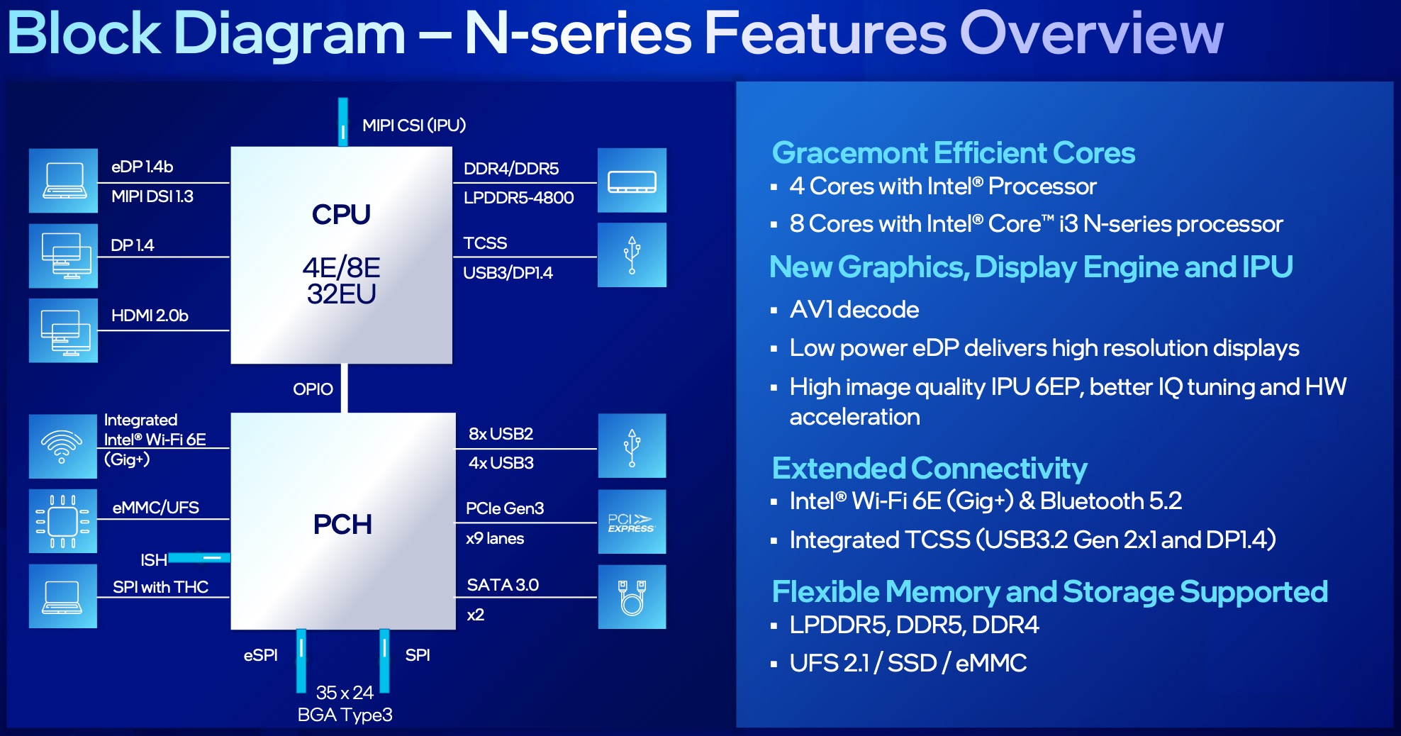
The Intel Core i3-N305 is an entry-level mobile CPU for thin and light laptops from the Alder Lake-N series. It was announced in early 2023 and offers no performance cores and 8 efficient cores (E-cores, Gracemont architecture). The chip does not support HyperThreading and clocks with up to 3.8 GHz (single core, 3 GHz all core Turbo). The performance of the E-cores should be similar to old Skylake cores (compare to the Core i7-6700HQ). All cores can use up to 6 MB L3-cache.
Performance
The performance depends on the cooling and TDP settings and should be somewhere similar to the old Alder Lake Pentium 8500 (1 performance core, 4 efficiency cores, max. 4.4 GHz and 8 MB L3-cache). The multi-threaded performance should be quite good with the 8 cores but will suffer due to the low TDP. Single thread performance will suffer due to the missing P-cores and relatively low boost clock speeds.
Features
The Alder Lake-N chips only support single channel memory with up to DDR5-4800, DDR4-3200 or LPDDR5-4800. The chip also supports Quick Sync and AV1 decoding (most likely same engine as in Alder Lake). Furthermore, Wi-Fi 6E and Bluetooth 5.2 are partly integrated (but no Thunderbolt). External chips can be connected via PCIe Gen3 x9 (via the PCH).
The integrated graphics adapter is based on the Xe-architecture and offersall 32 EUs (Execution Units) operating at up to 1.25 GHz. In addition to the single channel memory, the gaming performance is very limited of the iGPU.
Power consumption
The i3 has a base power consumption of 7 W and is therefore even suited for fanless cooling. The CPU is built with a further improved 10nm SuperFin process at Intel (called Intel 7).
| Model | Intel Celeron N5100 | Intel Core i3-N300 | ||||||||||||||||||||||||||||||||||||||||||||||||||||||||
| Series | Intel Jasper Lake | Intel Alder Lake-N | ||||||||||||||||||||||||||||||||||||||||||||||||||||||||
| Codename | Jasper Lake | Alder Lake-N | ||||||||||||||||||||||||||||||||||||||||||||||||||||||||
| Series: Alder Lake-N Alder Lake-N |
|
| ||||||||||||||||||||||||||||||||||||||||||||||||||||||||
| Clock | 1100 - 2800 MHz | <=3800 MHz | ||||||||||||||||||||||||||||||||||||||||||||||||||||||||
| L2 Cache | 1.5 MB | |||||||||||||||||||||||||||||||||||||||||||||||||||||||||
| L3 Cache | 4 MB | 6 MB | ||||||||||||||||||||||||||||||||||||||||||||||||||||||||
| Cores / Threads | 4 / 4 | 8 / 8 8 x 3.8 GHz Intel Crestmont E-Core | ||||||||||||||||||||||||||||||||||||||||||||||||||||||||
| TDP | 6 Watt | 7 Watt | ||||||||||||||||||||||||||||||||||||||||||||||||||||||||
| Technology | 10 nm | 10 nm | ||||||||||||||||||||||||||||||||||||||||||||||||||||||||
| max. Temp. | 105 °C | 105 °C | ||||||||||||||||||||||||||||||||||||||||||||||||||||||||
| Socket | BGA1338 | |||||||||||||||||||||||||||||||||||||||||||||||||||||||||
| Features | DDR4-2933/LPDDR4x-2933 RAM, PCIe 3, GNA, MMX, SSE, SSE2, SSE3, SSSE3, SSE4.1, SSE4.2, VMX, SMEP, SMAP, EIST, TM1, TM2, Turbo, AES-NI, RDRAND, RDSEED, SHA | |||||||||||||||||||||||||||||||||||||||||||||||||||||||||
| iGPU | Intel UHD Graphics (Jasper Lake 24 EU) (350 - 800 MHz) | Intel UHD Graphics Xe 750 32EUs (Rocket Lake) ( - 1250 MHz) | ||||||||||||||||||||||||||||||||||||||||||||||||||||||||
| Architecture | x86 | x86 | ||||||||||||||||||||||||||||||||||||||||||||||||||||||||
| Announced | ||||||||||||||||||||||||||||||||||||||||||||||||||||||||||
| Manufacturer | ark.intel.com | ark.intel.com |

