 Deutsch
 English
 Español
 Français
 Italiano
 Nederlands
 Polski
 Português
 Русский
 Türkçe
 Svenska
 Chinese
 Magyar
Intel Arc A770 vs Intel Iris Xe Graphics G7 96EUs vs Intel Arc A350M
Intel Arc A770
► remove from comparison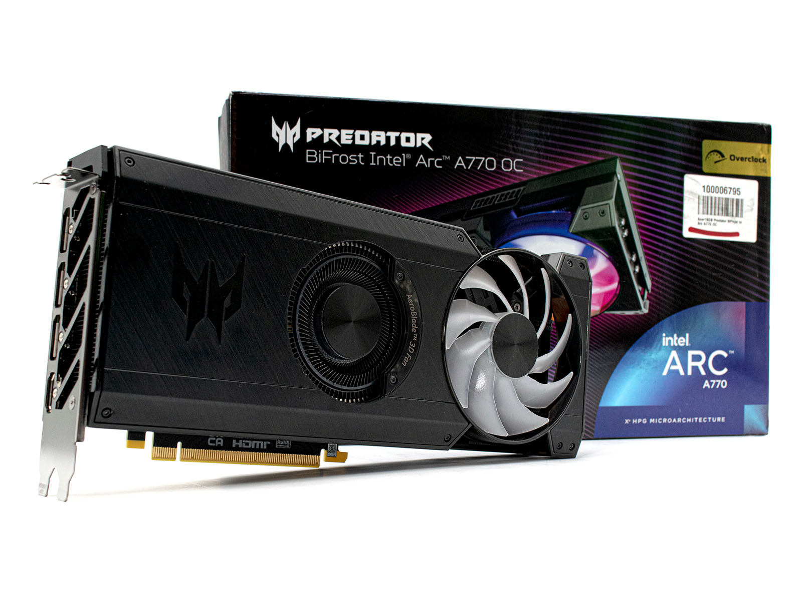
The Intel Arc A770 is a mid-range desktop GPU and is manufactured using the 6 nm process at TSMC. The graphics processor has 4,096 shader units and 8 or 16 GB GDDR6 VRAM with a 256-bit interface (16 Gbps, 512 GB/s).
Features
As the top model based on the Alchemist architecture, Intel offers the Arc A770, the top model in the series. As a completely new development, Intel wants to put pressure on AMD and Nvidia with these graphics cards. Features such as ray tracing are supported and the Intel Arc A770 comes with 32 RT cores. Intel is also implementing 512 Tensor Cores, which we can already find in the current graphics cards from Nvidia. With support for AV1, the graphics card is particularly interesting for content creators. Only the Ada Lovelace models from Nvidia and the RDNA3 GPUs from AMD are currently capable of hardware-side encoding and decoding with the new codec.
Performance
The performance of the Intel Arc A770 is comparable with an Nvidia GeForce RTX 4060 or an AMD Radeon RX 7600 comparable. The Intel model copes much better with newer games. With ray tracing enabled, the Intel Arc A770 can even outperform its two competitors. Based on the performance shown, the Intel Arc A770 is ideally suited for 1080p gaming in 2023.
Power consumption
The manufacturer specifies the power consumption of the Intel Arc A770 at 225 watts (TGP). This is slightly more than a Nvidia GeForce RTX 4060 or the AMD Radeon RX 7600.
Intel Iris Xe Graphics G7 96EUs
► remove from comparisonThe Intel Xe Graphics G7 (Tiger-Lake U GPU with 96 EUs) is a integrated graphics card in the high end Tiger-Lake U CPUs (15 - 28 Watt). It is using the new Xe architecture (Gen12) and was introduced in September 2020. The GPU clocks with a base clock speed (guaranteed) of 400 MHz in all CPUs and can boost up to 1340 MHz (i7-1185G7). The slowest variant offers only 1100 MHz boost (i5-1130G7, 12 Watt TDP).
The performance depends on the TDP settings of the laptop and the used cooling. First informations show that the chip can be configured at 12 and 28 Watt TDP default (as the Ice Lake-U chips) and the performance should be around a dedicated GeForce MX350 in 3DMark benchmarks. For gaming we are expecting a bit worse performance due to the missing dedicated graphics memory and driver support. Many games e.g. had problems when testing the various laptops (e.g. Horizon Zero Dawn or Cyberpunk 2077 did not start or were crashing - see list below). Less demanding games like the Mass Effect Legendary Edition ran in medium settings fine. Compared to the older Ice Lake Iris Plus G7 GPU, the new Tiger Lake GPU should be approximately twice as fast. Therefore, the iGPU is still only for lowest graphical settings and low resolutions in demanding games.
The Tiger Lake SoCs and therefore the integrated GPU are manufactured in the modern 10nm+ (10nm SuperFin) process (improved 10nm process) at Intel and therefore should offer a very good efficiency.
Intel Arc A350M
► remove from comparison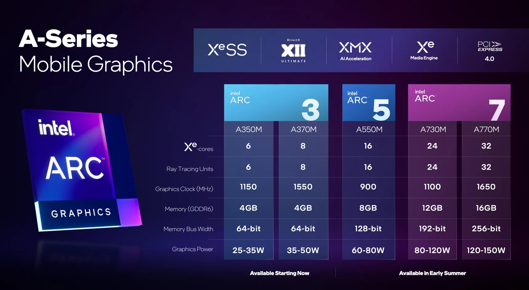
The Intel Arc A350M is a dedicated mobile entry level graphics card for laptops based on Xe HPG microarchitecture. It uses the ACM-G11 chip and offers 6 of the 8 Xe-cores (95 ALUs), 6 of the 8 ray tracing units and a 64-bit memory bus for 4 GB GDDR6 graphics memory. The chip integrates 7.2 billion transistors and the die measures 157 mm2.
The chip also integrates two media engines for VP9, AVC, HEVC, and AV1 8k en- and decoding. The 4 display pipes support up to 4x 4k120 HDR via DMI 2.0B or DisplayPort 2.0 10G.
The A350M is produced in 6nm at TSMC (N6 process) and supports dynamic power share (using Deep Link) with 12th gen Intel CPUs (Alder Lake).
| Intel Arc A770 | Intel Iris Xe Graphics G7 96EUs | Intel Arc A350M | ||||||||||||||||||||||||||||||||||||||||||||||||||||||||||||||||||||||||||||||||||||||||||||||||||||
| Arc Series |
|
|
| |||||||||||||||||||||||||||||||||||||||||||||||||||||||||||||||||||||||||||||||||||||||||||||||||||
| Codename | DG2-512 | Tiger Lake Xe | Alchemist | |||||||||||||||||||||||||||||||||||||||||||||||||||||||||||||||||||||||||||||||||||||||||||||||||||
| Architecture | Alchemist | Gen. 11 Ice Lake | Xe HPG | |||||||||||||||||||||||||||||||||||||||||||||||||||||||||||||||||||||||||||||||||||||||||||||||||||
| Pipelines | 4096 - unified | 96 - unified | 6 - unified | |||||||||||||||||||||||||||||||||||||||||||||||||||||||||||||||||||||||||||||||||||||||||||||||||||
| TMUs | 256 | |||||||||||||||||||||||||||||||||||||||||||||||||||||||||||||||||||||||||||||||||||||||||||||||||||||
| ROPs | 128 | |||||||||||||||||||||||||||||||||||||||||||||||||||||||||||||||||||||||||||||||||||||||||||||||||||||
| Raytracing Cores | 32 | 6 | ||||||||||||||||||||||||||||||||||||||||||||||||||||||||||||||||||||||||||||||||||||||||||||||||||||
| Tensor / AI Cores | 512 | |||||||||||||||||||||||||||||||||||||||||||||||||||||||||||||||||||||||||||||||||||||||||||||||||||||
| Core Speed | 2100 - 2400 (Boost) MHz | 400 - 1350 (Boost) MHz | 1150 MHz | |||||||||||||||||||||||||||||||||||||||||||||||||||||||||||||||||||||||||||||||||||||||||||||||||||
| Theoretical Performance | 39.32 TFLOPS FP16, 19.66 TFLOPS FP32 | |||||||||||||||||||||||||||||||||||||||||||||||||||||||||||||||||||||||||||||||||||||||||||||||||||||
| Cache | L2: 16 MB | L1: 1.1 MB, L2: 4 MB | ||||||||||||||||||||||||||||||||||||||||||||||||||||||||||||||||||||||||||||||||||||||||||||||||||||
| Memory Speed | 16000 effective = 2000 MHz | 14000 MHz | ||||||||||||||||||||||||||||||||||||||||||||||||||||||||||||||||||||||||||||||||||||||||||||||||||||
| Memory Bus Width | 256 Bit | 64 Bit | ||||||||||||||||||||||||||||||||||||||||||||||||||||||||||||||||||||||||||||||||||||||||||||||||||||
| Memory Type | GDDR6 | GDDR6 | ||||||||||||||||||||||||||||||||||||||||||||||||||||||||||||||||||||||||||||||||||||||||||||||||||||
| Max. Amount of Memory | 16 GB | 4 GB | ||||||||||||||||||||||||||||||||||||||||||||||||||||||||||||||||||||||||||||||||||||||||||||||||||||
| Shared Memory | no | yes | no | |||||||||||||||||||||||||||||||||||||||||||||||||||||||||||||||||||||||||||||||||||||||||||||||||||
| Memory Bandwidth | 512 GB/s | 112 GB/s | ||||||||||||||||||||||||||||||||||||||||||||||||||||||||||||||||||||||||||||||||||||||||||||||||||||
| API | DirectX 12 Ultimate (12_2), Shader 6.6, OpenGL 4.6, OpenCL 3.0, Vulkan 1.3 | DirectX 12_1, OpenGL 4.6 | DirectX 12_2, OpenGL 4.6, Vulkan 1.3 | |||||||||||||||||||||||||||||||||||||||||||||||||||||||||||||||||||||||||||||||||||||||||||||||||||
| Power Consumption | 225 Watt | 28 Watt | 35 Watt (25 - 35 Watt TGP) | |||||||||||||||||||||||||||||||||||||||||||||||||||||||||||||||||||||||||||||||||||||||||||||||||||
| Transistors | 21.7 Billion | 7.2 Billion | ||||||||||||||||||||||||||||||||||||||||||||||||||||||||||||||||||||||||||||||||||||||||||||||||||||
| Die Size | 406 mm² | 157 mm² | ||||||||||||||||||||||||||||||||||||||||||||||||||||||||||||||||||||||||||||||||||||||||||||||||||||
| technology | 6 nm | 10 nm | 6 nm | |||||||||||||||||||||||||||||||||||||||||||||||||||||||||||||||||||||||||||||||||||||||||||||||||||
| PCIe | 4.0 x16 | 4 8x | ||||||||||||||||||||||||||||||||||||||||||||||||||||||||||||||||||||||||||||||||||||||||||||||||||||
| Displays | 4 Displays (max.), HDMI 2.1, DisplayPort 2.0 | 4 Displays (max.), HDMI 2.0b, DisplayPort 2.0 10G Ready | ||||||||||||||||||||||||||||||||||||||||||||||||||||||||||||||||||||||||||||||||||||||||||||||||||||
| Date of Announcement | 12.10.2022 | 15.08.2020 | 30.03.2022 | |||||||||||||||||||||||||||||||||||||||||||||||||||||||||||||||||||||||||||||||||||||||||||||||||||
| Features | QuickSync | |||||||||||||||||||||||||||||||||||||||||||||||||||||||||||||||||||||||||||||||||||||||||||||||||||||
| Link to Manufacturer Page | ark.intel.com |
| ||||||||||||||||||||||||||
