The Apple A10X Fusion is a system on a chip (SoC) from Apple that is built into the 2017 iPad Pro models. It integrates six 64 Bit cores that are divided in two clusters. Three high performance cores are clocked at up to 2.39 GHz. The three power saving cores are used for non demanding tasks. It looks like only one of both clusters is able to run at a time (therefore the apps see only three cores). The principle is similar to the first generation of ARMs big.LITTLE concept.
The performance of the SoC is positioned in the high and and clearly faster than all previous Apple SoCs. Even compared to Android high-end SoCs like the Snapdragon 835, the A10X takes the lead (e.g. in Geekbench or Antutu).
According to TechInsights, the A10X is manufactured in the brand new 10 nm FinFet process at TSMC. Altough it offers more function blocks, the A10X is with measured 96.4 mm2 significantly smaller than the previous A9X (143.9 mm2).
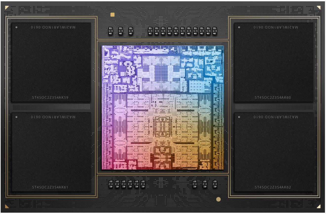
The Apple M2 Max is a System on a Chip (SoC) from Apple that is found in the early 2023 MacBook Pro 14 and 16-inch models. It offers all 12 CPU cores available in the chip divided in eight performance cores (P-cores) and four power-efficiency cores (E-cores). The E-cores clock with up to 3.4 GHz, the P-Cores up to 3.7 GHz (mostly 3.3 GHz in multi-threaded workloads and 3.4 GHz in single threaded).
The big cores (codename Avalanche) offer 192 KB instruction cache, 128 KB data cache, and 36 MB shared L2 cache (up from 24 MB in the M1 Pro). The four efficiency cores (codename Blizzard) are a lot smaller and offer only 128 KB instruction cache, 64 KB data cache, and 4 MB shared cache. CPU and GPU can both use the 49 MB SLC (System Level Cache).
The unified memory (32, 64, or 96 GB LPDDR5-6400) next to the chip is connected by a 512 Bit memory controller (400 GB/s bandwidth) and can be used by the GPU and CPU.
The CPU performance should be quite similar to the M2 Pro as only the higher memory bandwidth and bigger L3 cache could make a difference for some workloads.
Furthermore, the SoC integrates a fast 16 core neural engine (faster than M1 Max), a secure enclave (e.g., for encryption), a unified memory architecture, Thunderbolt 4 controller, an ISP, and media de- and encoders (including ProRes).
The M2 Max is manufactured in 5 nm at TSMC (second generation) and integrates 40 billion transistors. The power consumption of the CPU part is up to 36 Watt according to powermetrics. When fully loading the CPU and GPU cores, the chip uses up to 89 Watt and the CPU part is limited to 25 Watt.
- Range of benchmark values for this graphics card - Average benchmark values for this graphics card * Smaller numbers mean a higher performance 1 This benchmark is not used for the average calculation
v1.28
log 04. 18:19:06
#0 checking url part for id 9162 +0s ... 0s
#1 checking url part for id 14975 +0s ... 0s
#2 redirected to Ajax server, took 1720109946 +0s ... 0s
#3 did not recreate cache, as it is less than 5 days old! Created at Thu, 04 Jul 2024 05:15:21 +0200 +0s ... 0s
#4 composed specs +0.005s ... 0.005s
#5 did output specs +0s ... 0.005s
#6 getting avg benchmarks for device 9162 +0.001s ... 0.006s
#7 got single benchmarks 9162 +0.005s ... 0.01s
#8 getting avg benchmarks for device 14975 +0.001s ... 0.011s
#9 got single benchmarks 14975 +0.004s ... 0.015s
#10 got avg benchmarks for devices +0s ... 0.015s
#11 min, max, avg, median took s +0.013s ... 0.028s
 Deutsch
 English
 Español
 Français
 Italiano
 Nederlands
 Polski
 Português
 Русский
 Türkçe
 Svenska
 Chinese
 Magyar