 Deutsch
 English
 Español
 Français
 Italiano
 Nederlands
 Polski
 Português
 Русский
 Türkçe
 Svenska
 Chinese
 Magyar
Intel Core i5-540M vs Intel Processor U300
Intel Core i5-540M
► remove from comparison
The Intel Core i5-540M is a mid-range dual core CPU for laptops and clocks (due to the Turbo Mode) from 2.53 to 3.06 GHz. Each core is based on the Nehalem (Westmere) micro-architecture. Hyperthreading enables the Dual Core CPU to handle 4 threads at once (for a better usage of the pipeline). Compared to the faster Core i7-620M, the 540M only has 3 MB Level 3 Cache and a lower clock speed.
A feature of the new Core i5-540M is the integrated graphics card called GMA HD and memory controller. Both are on a separate die that is still manufactured in 45nm whereas the CPU die is already manufactured in the new 32nm process.
The performance of the Core i5-540M is on average faster than a 2.8 GHz Core 2 Duo T9800 and in some benchmarks even faster than the fastest Core 2 Duo T9900 (e.g. 3DMark 06 CPU Score). Therefore, the Core i5-540M is a high end dual core cpu which should handle all daily work and gaming tasks. Only the quad core i7 CPUs can be noticeably faster at tasks that require four or more threads (e.g. rendering).
The 32nm cpu cores of the Westmere generation can also process some new instructions to accelerate AES encryptions.
The integrated Intel Graphics Media Accelerator HD (GMA HD) graphics card is known to be clocked up to 500-766 MHz and should be clearly faster than the old GMA 4500MHD. A GeForce 9400M (ION) should still be a faster (especially as Nvidia and ATI cards have a better driver support than Intel up to now). According to rumors, the GMA core will also use the Turbo Mode regulate the clock speed.
The power consumption of 35 Watt TDP (max.) counts for the whole package and therefore it is clearly better than the 35 Watt TDP of the Core 2 Duo T-series (CPU alone). Due to the Turbo Boost, the Core i5 is likely to use the whole TDP of 35 Watt under load and therefore can use more power than a similar specified Core 2 Duo. In Idle mode, the i5 uses clearly less power than the Core 2 Duo CPUs.
Intel Processor U300
► remove from comparison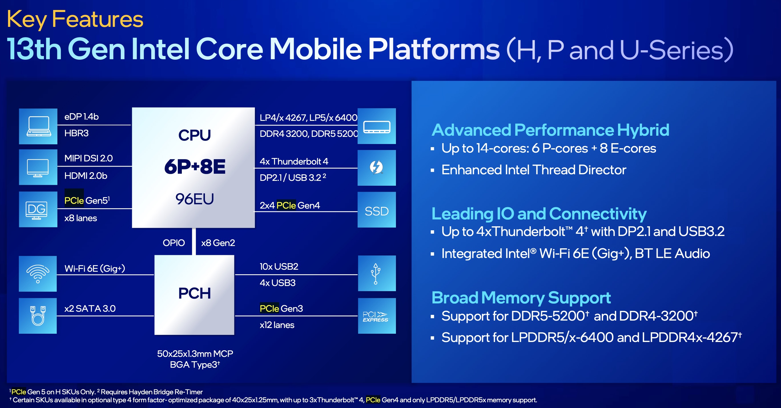
The Intel Processor U300 is an entry-level mobile CPU for thin and light laptops of the Raptor Lake-U series. It was announced in early 2023 and offers one performance core (Raptor Cove architecture P-core, similar to Alder Lake) and 4 efficient cores (E-cores, Gracemont architecture). The P-cores support Hyper-Threading for 6 processing threads when combined with the E-cores. The clock rate ranges from 1.2 to 4.4 GHz on the performance cluster and 0.9 to 3.3 GHz on the efficient cluster. The per-clock performance of the E-cores should be similar to old Skylake cores (compare to the Core i7-6700HQ). All cores have access to 8 MB of L3 cache.
Performance
While we have not tested a single system powered by the U300 as of February 2024, its performance should be very similar to the outgoing Alder Lake Pentium 8505, since there is little difference between the two. The average U300 is set to be 10% to 20% behind the Ryzen 3 5300U and the Core i7-1185G7, as far as multi-thread benchmark scores are concerned, making the former an entry-level chip as of early 2024.
Your mileage may vary depending on how high the CPU power limits are.
Features
The integrated memory controller supports various memory types up to DDR5-4800, DDR4-3200, LPDDR5-5200, and LPDDR4x-4267. The Thread Director (in hardware) can support the operating system to decide which thread to use on the performance or efficient cores for the best performance. For AI tasks, the CPU also integrates GNA 3.0 and DL Boost (via AVX2). Quick Sync in version 8 is the same as in the Rocket Lake CPUs and supports MPEG-2, AVC, VC-1 decode, JPEG, VP8 decode, VP9, HEVC, and AV1 decode in hardware. Several PCIe 4 lanes (x8 for a GPU and two x4 for SSDs) as well as several PCIe 3 lanes are on offer.
The integrated graphics adapter is based on the Xe architecture and offers 48 of the 96 EUs (Execution Units) operating at up to 1.1 GHz.
Power consumption
The U300 has a base power consumption of 15 W, with 55 W being its maximum Intel-recommended Turbo power consumption. The CPU is built with a 10 nm process marketed as Intel 7.
| Model | Intel Core i5-540M | Intel Processor U300 | ||||||||||||||||||||||||||||||||||||||||||||||||||||||||||||||||||||||||||||||||||||
| Series | Intel Core i5 | Intel Raptor Lake-U | ||||||||||||||||||||||||||||||||||||||||||||||||||||||||||||||||||||||||||||||||||||
| Codename | Arrandale | Raptor Lake-U | ||||||||||||||||||||||||||||||||||||||||||||||||||||||||||||||||||||||||||||||||||||
| Series: Raptor Lake-U Raptor Lake-U |
|
| ||||||||||||||||||||||||||||||||||||||||||||||||||||||||||||||||||||||||||||||||||||
| Clock | 2530 - 3066 MHz | 900 - 4400 MHz | ||||||||||||||||||||||||||||||||||||||||||||||||||||||||||||||||||||||||||||||||||||
| FSB | 2500 | |||||||||||||||||||||||||||||||||||||||||||||||||||||||||||||||||||||||||||||||||||||
| L1 Cache | 128 KB | 464 KB | ||||||||||||||||||||||||||||||||||||||||||||||||||||||||||||||||||||||||||||||||||||
| L2 Cache | 512 KB | 3.5 MB | ||||||||||||||||||||||||||||||||||||||||||||||||||||||||||||||||||||||||||||||||||||
| L3 Cache | 3 MB | 8 MB | ||||||||||||||||||||||||||||||||||||||||||||||||||||||||||||||||||||||||||||||||||||
| Cores / Threads | 2 / 4 | 5 / 6 1 x 4.4 GHz Intel Raptor Cove P-Core 4 x 3.3 GHz Intel Gracemont E-Core | ||||||||||||||||||||||||||||||||||||||||||||||||||||||||||||||||||||||||||||||||||||
| TDP | 35 Watt | 15 Watt | ||||||||||||||||||||||||||||||||||||||||||||||||||||||||||||||||||||||||||||||||||||
| Transistors | 382+177 Million | |||||||||||||||||||||||||||||||||||||||||||||||||||||||||||||||||||||||||||||||||||||
| Technology | 32 nm | 10 nm | ||||||||||||||||||||||||||||||||||||||||||||||||||||||||||||||||||||||||||||||||||||
| Die Size | 81+114 mm2 | |||||||||||||||||||||||||||||||||||||||||||||||||||||||||||||||||||||||||||||||||||||
| max. Temp. | 105 °C | 100 °C | ||||||||||||||||||||||||||||||||||||||||||||||||||||||||||||||||||||||||||||||||||||
| Socket | BGA1288, PGA988 | BGA1744 | ||||||||||||||||||||||||||||||||||||||||||||||||||||||||||||||||||||||||||||||||||||
| Features | Turbo Boost, Hyper Threading, Enhanced Speedstep, integrierte GMA HD 733MHz, | DDR4-3200/LPDDR4x-4267/DDR5-5200/LPDDR5-5200/LPDDR5x-5200 RAM, PCIe 4, Thr. Director, DL Boost, GNA, MMX, SSE, SSE2, SSE3, SSSE3, SSE4.1, SSE4.2, AVX, AVX2, BMI2, ABM, FMA, ADX, VMX, SMEP, SMAP, EIST, TM1, TM2, HT, Turbo, SST, AES-NI, RDRAND, RDSEED, SHA | ||||||||||||||||||||||||||||||||||||||||||||||||||||||||||||||||||||||||||||||||||||
| Architecture | x86 | x86 | ||||||||||||||||||||||||||||||||||||||||||||||||||||||||||||||||||||||||||||||||||||
| $257 U.S. | ||||||||||||||||||||||||||||||||||||||||||||||||||||||||||||||||||||||||||||||||||||||
| Announced | ||||||||||||||||||||||||||||||||||||||||||||||||||||||||||||||||||||||||||||||||||||||
| Manufacturer | ark.intel.com | ark.intel.com | ||||||||||||||||||||||||||||||||||||||||||||||||||||||||||||||||||||||||||||||||||||
| TDP Turbo PL2 | 55 Watt | |||||||||||||||||||||||||||||||||||||||||||||||||||||||||||||||||||||||||||||||||||||
| iGPU | Intel UHD Graphics Xe G4 48EUs ( - 1100 MHz) |

