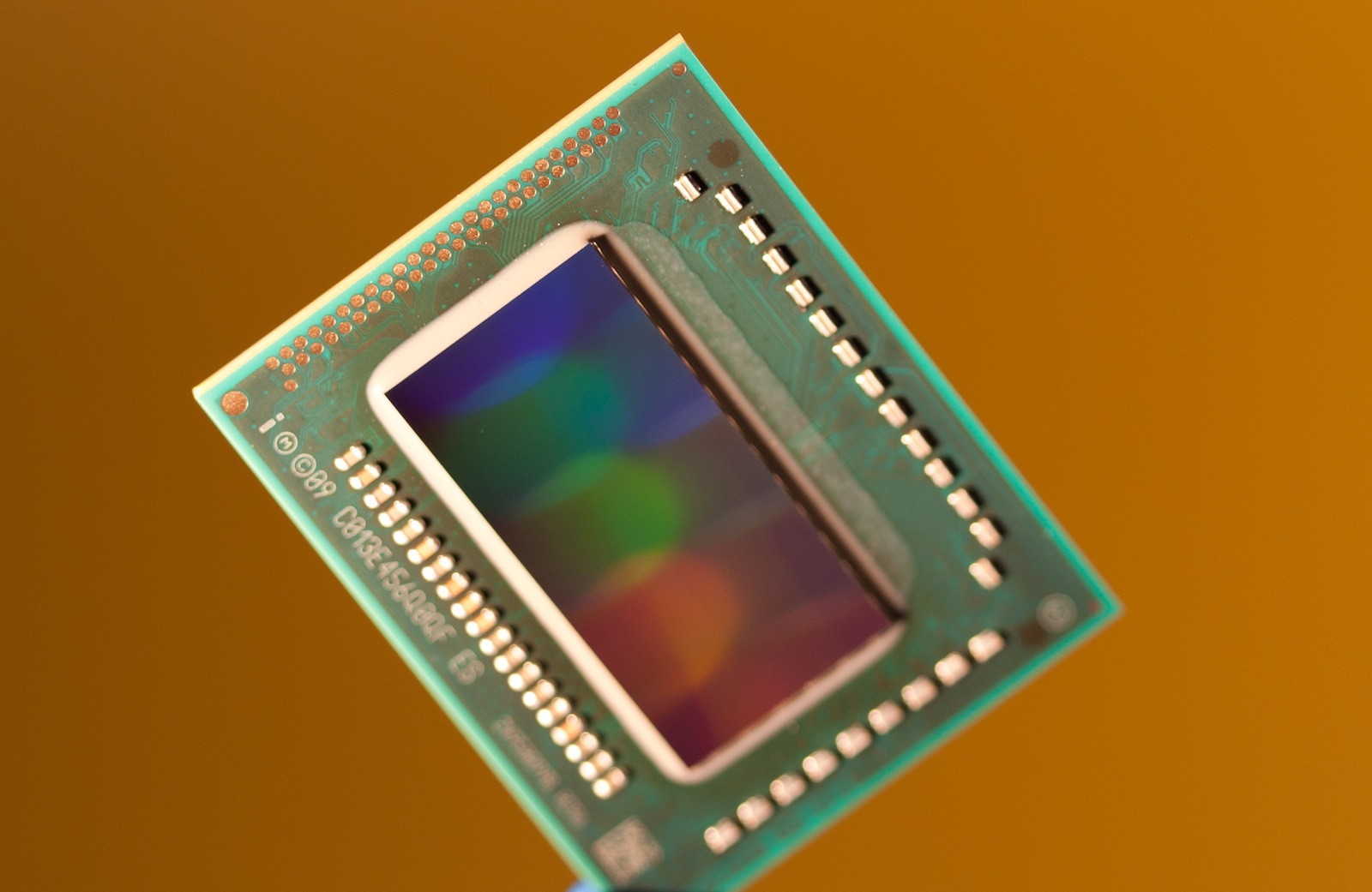
The Intel Core i7-2640M is the fastest dual core processor at the time of introduction in Q3 2011 and successor of the slower clocked i7-2620M. It is based on the Sandy Bridge architecture and offers Hyperthreading to handle 4 threads at once (for a better usage of the pipeline). Compared to the slower Core i5, the i7 offers a larger last level cache of 4MB. The base clock speed is 2.8 GHz but due to Turbo Boost it can reach 3.3 GHz (2 cores active) and 3.5 GHz (1 core active).
Sandy Bridge is the evolutionary successor of the Arrandale architecture. The most noteable improvements are the new 256Bit AVX instructions, the improved Turbo 2.0 and the integration of the graphics card into the 32nm CPU core.
Der i7-2640M offers an integrated graphics card ( Intel HD Graphics 3000) which is clearly faster then the older Intel HD Graphics in the Arrandale CPUs. As the new GPU is included in the CPU, it is also manufactured in 32nm and shares the fast level 3 cache with the CPU cores (using a new ring bus). In the 2620M it is clocked from 650-1300MHz (Turbo Boost), and in the 2640M it should be similar.
Furthermore, an improved dual-channel DDR3 memory controller is included on the CPU die that is used by the CPU and GPU part.
Due to the improved architecture and the new Turbo Boost 2.0, the average performance of the Core i7-2640M is higher than a similar clocked Arrandale Core i7 dual core. The performance should even excel the old high-end quad core models like the Core i7-820QM.
The 35W TDP rating includes the integrated GPU and memory controller.
The Intel Core 2 Duo P9500 was a upper middle class dual core CPU for laptops, at the time of introduction. It is similar to the Core 2 Duo T9400 except for the lower TDP of 25 versus 35 Watt).
Due to the relatively high clock speed and 6MB Level 2 cache, the P9500 offers enough performance for most demanding games (in 2009) and applications.
The P9500 uses a Penryn (Montevina Update) core that features 2 integer units, 1 floating point unit, 1 load unit, and 1 store unit in a 14-stages long pipeline. Due to the Wide Dynamic Execution Technology, the core is able to simultaneously execute up to four instructions.
The integrated Enhanced Speedstep is able to downclock the core dynamically to save power (in idle mode).
The Intel Core 2 Duo P8400 is a dual core processor for laptops. It features 2.26 GHz and a shared level 2 cache of 3 MB. Due to the smaller cache (Core 2 Duo T-Models got usually 6 MB at this clock rate), the TDP is only 25 Watt (instead of the 35 Watt of the T-models).
The performance of the P8400 is on par with the fast Turion II Ultra with about 2.4 to 2.6 GHz. Modern demanding games like Supreme Commander may be limited by the CPU performance. High end gamers should choose a higher clocked Core 2 Duo (or Core i5 / i7).
The P8400 uses a Penryn (Montevina Update) core that features 2 integer units, 1 floating point unit, 1 load unit, and 1 store unit in a 14-stages long pipeline. Due to the Wide Dynamic Execution Technology, the core is able to simultaneously execute up to four instructions.
The integrated Enhanced Speedstep is able to downclock the core dynamically as low as 800 MHz to save power (in idle mode).
The Core 2 Duo P8400 can be used in a Socket P socket with 479 pins: Socket P / Micro Flip-Chip Pin Grid Array (Micro-FCPGA) requires 479-pin surface mount Zero Insertion Force (ZIF) socket (mPGA479M socket) or Micro Flip-Chip Ball Grid Array (Micro-FCBGA) for surface mount (479-ball)
Average Benchmarks Intel Core 2 Duo P9500 → 70%n=10
Average Benchmarks Intel Core 2 Duo P8400 → 66%n=10
- Range of benchmark values for this graphics card - Average benchmark values for this graphics card * Smaller numbers mean a higher performance 1 This benchmark is not used for the average calculation
v1.28
log 02. 17:13:06
#0 checking url part for id 2839 +0s ... 0s
#1 checking url part for id 405 +0s ... 0s
#2 checking url part for id 398 +0s ... 0s
#3 redirected to Ajax server, took 1719933186 +0s ... 0s
#4 did not recreate cache, as it is less than 5 days old! Created at Mon, 01 Jul 2024 05:15:43 +0200 +0s ... 0s
#5 composed specs +0.008s ... 0.008s
#6 did output specs +0s ... 0.008s
#7 getting avg benchmarks for device 2839 +0.001s ... 0.009s
#8 got single benchmarks 2839 +0.013s ... 0.022s
#9 getting avg benchmarks for device 405 +0.001s ... 0.023s
#10 got single benchmarks 405 +0.005s ... 0.028s
#11 getting avg benchmarks for device 398 +0.001s ... 0.028s
#12 got single benchmarks 398 +0.025s ... 0.054s
#13 got avg benchmarks for devices +0s ... 0.054s
#14 min, max, avg, median took s +0.022s ... 0.076s
 Deutsch
 English
 Español
 Français
 Italiano
 Nederlands
 Polski
 Português
 Русский
 Türkçe
 Svenska
 Chinese
 Magyar